Micron Announces 176-layer 3D NAND
by Billy Tallis on November 9, 2020 4:00 PM EST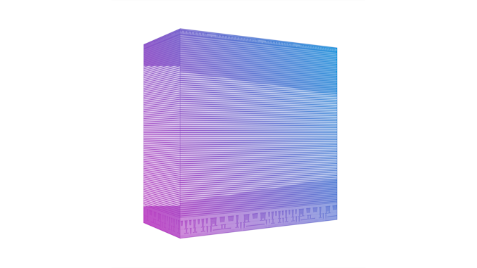
Just in time for Flash Memory Summit, Micron is announcing their fifth generation of 3D NAND flash memory, with a record-breaking 176 layers. The new 176L flash is their second generation developed since the dissolution of Micron's memory collaboration with Intel, after which Micron switched from a floating-gate memory cell design to a charge-trap cell. Micron's previous generation 3D NAND was a 128-layer design that served as a short-lived transitional node for them to work out any issues with the switch to charge trap flash. Micron's 128L flash has had minimal presence on the market, so their new 176L flash will in many cases serve as the successor to their 96L 3D NAND as well.
Micron is still withholding many technical details about their 176L NAND, with more information planned to be shared at the end of the month. But for now, we know their first 176L parts are 512Gbit TLC dies, built using string stacking of two 88-layer decks—Micron would seem to now be in second place behind Samsung for how many layers of NAND flash memory cells they can fabricate at a time, and clearly in first place for the total number of layers on a die.
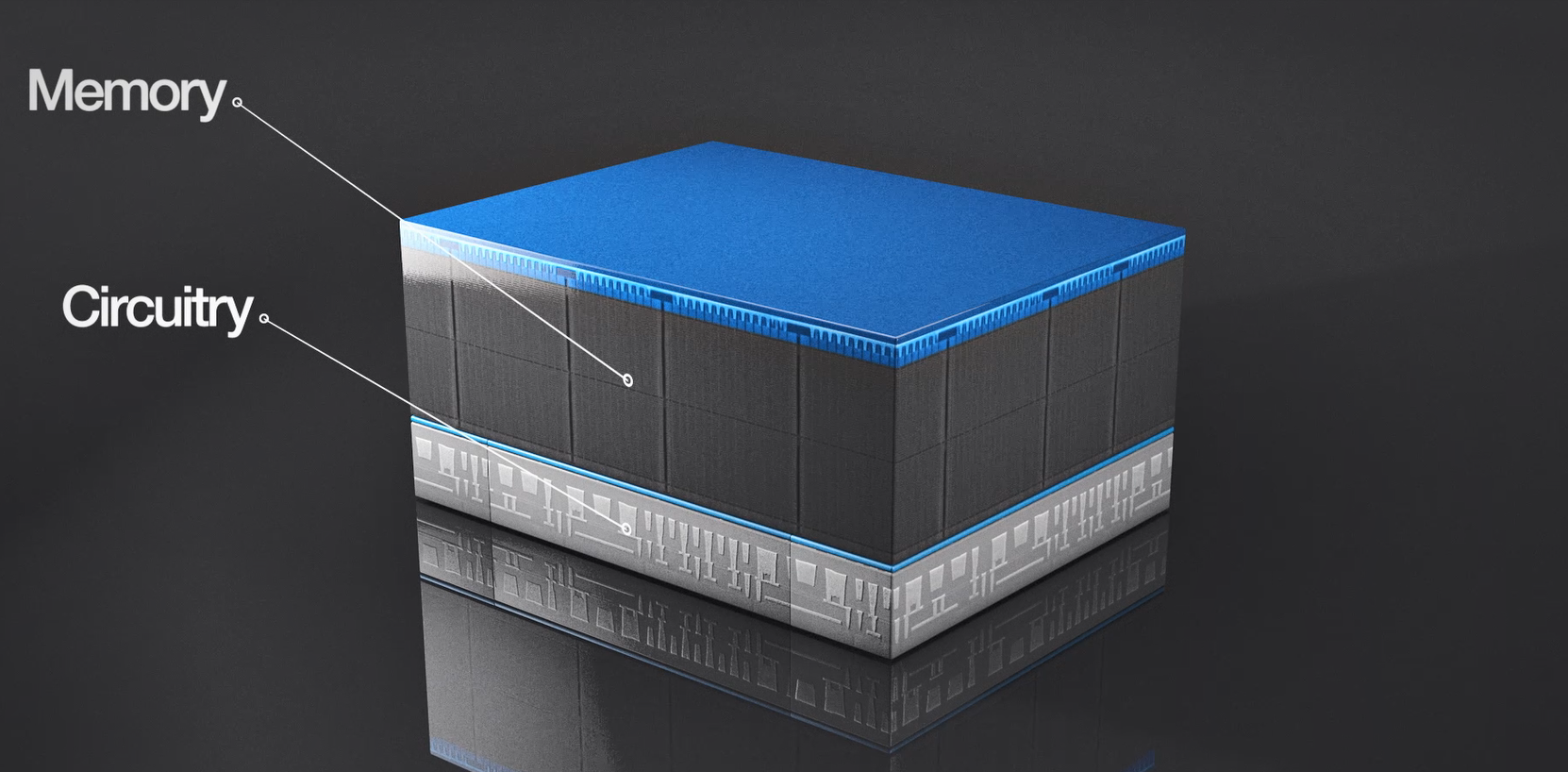
The switch to a replacement gate/charge trap cell design seems to have enabled a significant reduction in layer thickness: the 176L dies are 45µm thick, about the same total thickness as Micron's 64L floating-gate 3D NAND. A 16-die stacked package comes in at less than 1.5mm thick, suitable for most mobile and memory card use cases. As with previous generations of Micron 3D NAND, the chip's peripheral logic is mostly fabricated under the NAND memory cell stacks, a technology Micron calls "CMOS under Array" (CuA). This has repeatedly helped Micron deliver some of the smallest die sizes, and Micron estimates their 176L 512Gbit die is about 30% smaller than the best their competitors currently offer.
The 176L NAND supports an interface speed of 1600MT/s, up from 1200MT/s for their 96L and 128L flash. Read and write (program) latency are both improved by over 35% compared to their 96L NAND, or by over 25% compared to their 128L NAND. Micron cites an overall mixed workload improvement of about 15% for compared to their UFS 3.1 modules using 96L NAND.
Micron's 176L 3D NAND has already started volume production and is shipping in some Crucial-branded consumer SSD products. However, Micron hasn't specified which specific Crucial products are now using 176L NAND (or their 128L NAND, for that matter), so we expect that this is a fairly low-volume release for now. Still, over the next year we should 176L NAND production ramp up to higher volumes than their 128L process ever reached, and we can expect a wide range of products based on this 176L NAND to be released and replace most of what's using their 96L NAND.


29 Comments
View All Comments
yeeeeman - Tuesday, November 10, 2020 - link
just...go to 1k layers so we can reach the 1pb mark tomorrow.TheWereCat - Tuesday, November 10, 2020 - link
3 slot NAND?nandnandnand - Tuesday, November 10, 2020 - link
They could probably put 1 PB in a 3.5" drive soon if they wanted to (3.5" HDD volume ÷ microSD volume ≥ 2000). Whenever it is available, you will be using 16 TB, at best. Cost is the problem, not capacity.AlexDaum - Friday, November 13, 2020 - link
Also, memory controller and speed is a problem. For a useful 1PB SSD you would need a fast controller, it won't be useful at all with SATA or even SAS speed. With SATA and 600MB/s sequencial write speed it will take over 19 days to fill that drive!There is already the Nimbus ExaDrive 100TB 3.5" SSD, getting another 10x density improvement might be possible with new high layer NAND chips, thinner PCBs and tighter stacking
RSAUser - Saturday, November 14, 2020 - link
1PB / 32GBps = ~8.5 hours on a maxed out PCIe 4 16x lane.Don't think there's really a market for that yet.
rpg1966 - Tuesday, November 10, 2020 - link
Question from a dummy:What's the difference between "stacking of two 88-layer decks" into a 176-layer die, versus stacking 16 of those dies into a package?
AlexDaum - Friday, November 13, 2020 - link
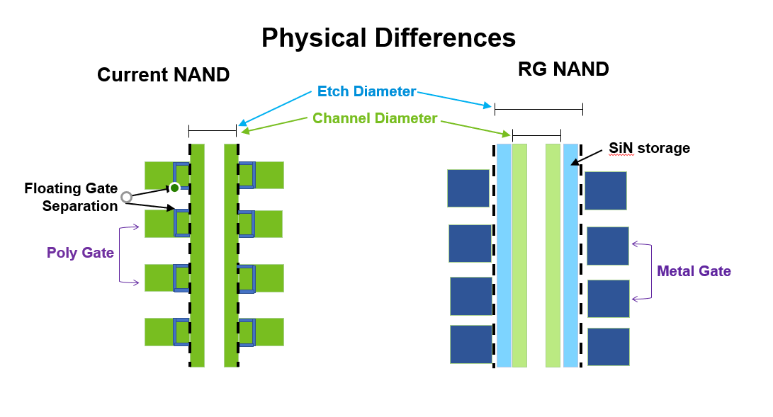
As I understand it, each deck has a continuous Channel + SiN for storing the data and separate gates. It seems they can't make that channel tall enough for all layers, so they fab it in 2 steps, but still on the same wafer, probably with some kind of metal interconnect between the decks.For stacking the dies in a package the wafer is first sawed into dies and those are connected to each other with some kind of interconnect, probably using TSVs (Through silicon vias). After stacking all the dies, the chip is then bonded onto some kind of carrier for the BGA package and molded in plastic.
Rictorhell - Wednesday, February 17, 2021 - link
Can anyone speculate IF Micron or Crucial were to release a single or double sided 2230 m.2 ssd, using this 176 layer technology, what the potential capacity of either one of those drives MIGHT be?Rictorhell - Wednesday, February 17, 2021 - link
Assuming that they were willing to max out the capacity of said SSD, using this current technology?