The Apple A15 SoC Performance Review: Faster & More Efficient
by Andrei Frumusanu on October 4, 2021 9:30 AM EST- Posted in
- Mobile
- Apple
- Smartphones
- Apple A15
A few weeks ago, we’ve seen Apple announce their newest iPhone 13 series devices, a set of phones being powered by the newest Apple A15 SoC. Today, in advance of the full device review which we’ll cover in the near future, we’re taking a closer look at the new generation chipset, looking at what exactly Apple has changed in the new silicon, and whether it lives up to the hype.
This year’s announcement of the A15 was a bit odder on Apple’s PR side of things, notably because the company generally avoided making any generational comparisons between the new design to Apple’s own A14. Particularly notable was the fact that Apple preferred to describe the SoC in context of the competition; while that’s not unusual on the Mac side of things, it was something that this year stood out more than usual for the iPhone announcement.
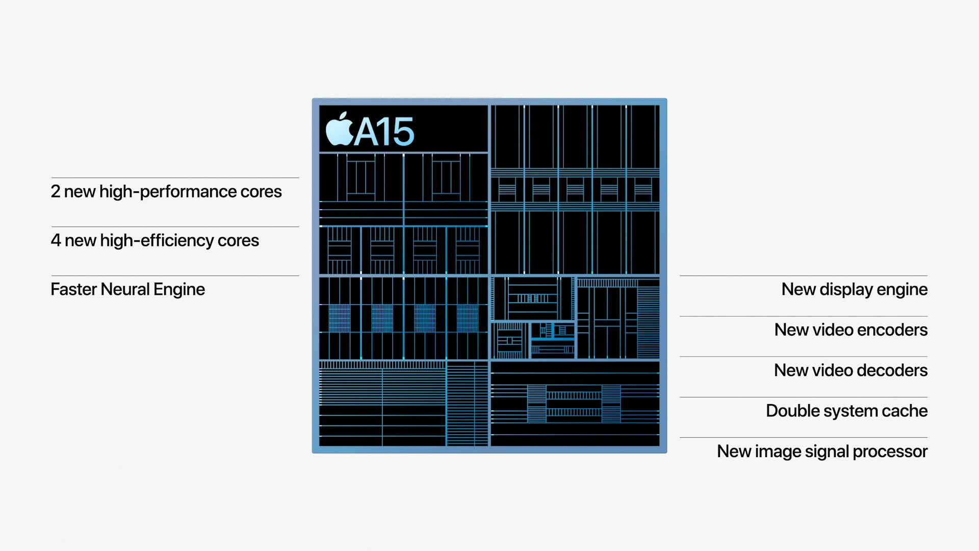
The few concrete factoids about the A15 were that Apple is using new designs for their CPUs, a faster Neural engine, a new 4- or 5-core GPU depending on the iPhone variant, and a whole new display pipeline and media hardware block for video encoding and decoding, alongside new ISP improvements for camera quality advancements.
On the CPU side of things, improvements were very vague in that Apple quoted to be 50% faster than the competition, and the GPU performance metrics were also made in such a manner, describing the 4-core GPU A15 being +30% faster than the competition, and the 5-core variant being +50% faster. We’ve put the SoC through its initial paces, and in today’s article we’ll be focusing on the exact performance and efficiency metrics of the new chip.
Frequency Boosts; 3.24GHz Performance & 2.0GHz Efficiency Cores
Starting off with the CPU side of things, the new A15 is said to feature two new CPU microarchitectures, both for the performance cores as well as the efficiency cores. The first few reports about the performance of the new cores were focused around the frequencies, which we can now confirm in our measurements:
| Maximum Frequency vs Loaded Threads Per-Core Maximum MHz |
||||||
| Apple A15 | 1 | 2 | 3 | 4 | ||
| Performance 1 | 3240 | 3180 | ||||
| Performance 2 | 3180 | |||||
| Efficiency 1 | 2016 | 2016 | 2016 | 2016 | ||
| Efficiency 2 | 2016 | 2016 | 2016 | |||
| Efficiency 3 | 2016 | 2016 | ||||
| Efficiency 4 | 2016 | |||||
| Maximum Frequency vs Loaded Threads Per-Core Maximum MHz |
||||||
| Apple A14 | 1 | 2 | 3 | 4 | ||
| Performance 1 | 2998 | 2890 | ||||
| Performance 2 | 2890 | |||||
| Efficiency 1 | 1823 | 1823 | 1823 | 1823 | ||
| Efficiency 2 | 1823 | 1823 | 1823 | |||
| Efficiency 3 | 1823 | 1823 | ||||
| Efficiency 4 | 1823 | |||||
Compared to the A14, the new A15 increases the peak single-core frequency of the two-performance core cluster by 8%, now reaching up to 3240MHz compared to the 2998MHz of the previous generation. When both performance cores are active, their operating frequency actually goes up by 10%, both now running at an aggressive 3180MHz compared to the previous generation’s 2890MHz.
In general, Apple’s frequency increases here are quite aggressive given the fact that it’s quite hard to push this performance aspect of a design, especially when we’re not expecting major performance gains on the part of the new process node. The A15 should be made on an N5P node variant from TSMC, although neither company really discloses the exact details of the design. TSMC claims a +5% frequency increase over N5, so for Apple to have gone further beyond this would have indicated an increase in power consumption, something to keep in mind of when we dive deeper into the power characteristics of the CPUs.
The E-cores of the A15 are now able to clock up to 2016MHz, a 10.5% increase over the A14’s cores. The frequency here is independent of the performance cores, as in the number of threads in the cluster doesn’t affect the other cluster, or vice-versa. Apple has done some more interesting changes to the little cores this generation, which we’ll come to in a bit.
Giant Caches: Performance CPU L2 to 12MB, SLC to Massive 32MB
One more straightforward technical detail Apple revealed during its launch was that the A15 now features double the system cache compared to the A14. Two years ago we had detailed the A13’s new SLC which had grown from 8MB in the A12 to 16MB, a size that was also kept constant in the A14 generation. Apple claiming they’ve doubled this would consequently mean it’s 32MB now in the A15.
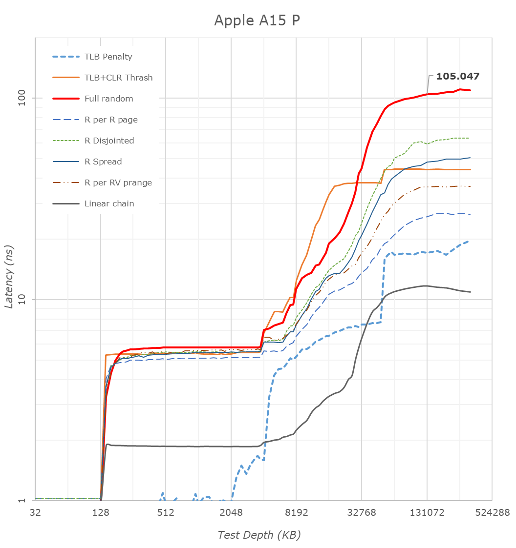
Looking at our latency tests on the new A15, we can indeed now confirm that the SLC has now doubled up to 32MB, further pushing the memory depth to reach DRAM. Apple’s SLC is likely to be a key factor in the power efficiency of the chip, being able to keep memory accesses on the same silicon rather than going out to slower, and more power inefficient DRAM. We’ve seen these types of last-level caches being employed by more SoC vendors, but at 32MB, the new A15 dwarfs the competition’s implementations, such as the 3MB SLC on the Snapdragon 888 or the estimated 6-8MB SLC on the Exynos 2100.
What Apple didn’t divulge, is also changes to the L2 cache of the performance cores, which has now grown by 50% from 8MB to 12MB. This was actually the same L2 size as on the Apple M1, only this time around it’s serving only two performance cores rather than four. The access latency appears to have risen from 16 cycles on the A14 to 18 cycles on the A15.
A 12MB L2 is again humongous, over double compared to the combined L3+L2 (4+1+3x0.5 = 6.5MB) of other designs such as the Snapdragon 888. It very much appears Apple has invested a lot of SRAM into this year’s SoC generation.
The efficiency cores this year don’t seem to have changed their cache sizes, remaining at 64KB L1D’s and 4MB shared L2’s, however we see Apple has increased the L2 TLB to 2048 entries, now covering up to 32MB, likely to facilitate better SLC access latencies. Interestingly, Apple this year now allows the efficiency cores to have faster DRAM access, with latencies now at around 130ns versus the +215ns on the A14, again something to keep in mind of in the next performance section of the article.
CPU Microarchitecture Changes: A Slow(er) Year?
This year’s CPU microarchitectures were a bit of a wildcard. Earlier this year, Arm had announced the new Armv9 ISA, predominantly defined by the new SVE2 SIMD instruction set, as well as the company’s new Cortex series CPU IP which employs the new architecture. Back in 2013, Apple was notorious for being the first on the market with an Armv8 CPU, the first 64-bit capable mobile design. Given that context, I had generally expected this year’s generation to introduce v9 as well, but however that doesn’t seem to be the case for the A15.
Microarchitecturally, the new performance cores on the A15 doesn’t seem to differ much from last year’s designs. I haven’t invested the time yet to look at every nook and cranny of the design, but at least the back-end of the processor is identical in throughput and latencies compared to the A14 performance cores.
The efficiency cores have had more changes, alongside some of the memory subsystem TLB changes, the new E-core now gains an extra integer ALU, bringing the total up to 4, up from the previous 3. The core for some time no longer could be called “little” by any means, and it seems to have grown even more this year, again, something we’ll showcase in the performance section.
The possible reason for Apple’s more moderate micro-architectural changes this year might be a storm of a few factors – Apple had notably lost their lead architect on the big performance cores, as well as parts of the design teams, to Nuvia back in 2019 (later acquired by Qualcomm earlier this year). The shift towards Armv9 might also imply some more work done on the design, and the pandemic situation might also have contributed to some non-ideal execution. We’ll have to examine next year’s A16 to really determine if Apple’s design cadence has slowed down, or whether this was merely just a slippage, or simply a lull before a much larger change in the next microarchitecture.
Of course, the tone here paints rather conservative improvement of the A15’s CPUs, which when looking at performance and efficiency, are anything but that.


204 Comments
View All Comments
Andrei Frumusanu - Monday, October 4, 2021 - link
I didn't see much difference on the Max. The issue is chip to body dissipation, not total body to ambient dissipation.cha0z_ - Monday, October 4, 2021 - link
Yeah, guessed that much, but still had hopes. Basically the sustained GPU performance is just a tad higher vs my 11 pro max and I am kinda sad about it even with all the other improvements. :(There are super good, but GPU demanding games like x-com 2 WOTC, not to mention for the 120Hz scenario, but even if more efficient the FPS number when you play for more than 10m will be indistinguishable if no FPS counter is visible.
Correct me if I am wrong and if not a big hassle given I really respect your opinion and work + you have experience with 11 pro max also - do you think it's a decent overall upgrade (simple yes/no will do. I am power user + got 2233rz 120Hz at launch :) ). Especially by feel how do you compare them in gaming?
Also cheers for your great articles and deep dives! Love them all!
repoman27 - Monday, October 4, 2021 - link
Not arguing one way or the other as to the merits of Apple's thermal solution, but the side of the A15 package which faces the interior of the PCB sandwich is a PoP with 4 SDRAM dies in it. The business side of the SoC is attached to a very thin PCB via InFO. The opposite side of the PCB in the region where the SoC is located has very little active circuitry other than the audio chips and secure element. However, it does have a can with thermal pads to help transfer the heat from the SoC upwards through the screen.In other words, I believe most of the heat from the SoC is radiated upwards through the screen / top of the device, while the heat from the modem / RF transceiver chips is radiated through the back glass / bottom of the device.
Andrei Frumusanu - Monday, October 4, 2021 - link
We can theorize, but at the end of the day it's got far lower sustained power than any other phone and there are thermal issues that Apple has encountered several times now, some not addressed in articles.repoman27 - Monday, October 4, 2021 - link
I have no idea if Apple made good decisions regarding thermals in this case or not, and I'm glad you're investigating / reporting on the topic. However, by constantly pushing density further than everyone else and using technologies like InFO and substrate-like PCBs, Apple may be solving for a slightly different set of problems than their competitors.teldar - Wednesday, October 6, 2021 - link
It's not really Apple pushing density. It's the processor manufacturer. That's a little misleading.Ppietra - Wednesday, October 6, 2021 - link
teldar, it’s both! It is up to Apple to decide which node it wants to use.Spunjji - Friday, October 8, 2021 - link
@Ppietra & teldar - I think repoman27 meant "pushing density" in terms of PCB layout and design, rather than the node the CPU is manufactured on.unclevagz - Monday, October 4, 2021 - link
How does the Spec 2017 performance here compare against x86 (Zen 3/RKL)?Andrei Frumusanu - Monday, October 4, 2021 - link
Comparative subsets would 5950X 7.29 int / 9.79 fp, 11900K 6.61 int / 9.58 fp. versus 7.28 / 10.15 on A15.