Google's Tensor inside of Pixel 6, Pixel 6 Pro: A Look into Performance & Efficiency
by Andrei Frumusanu on November 2, 2021 8:00 AM EST- Posted in
- Mobile
- Smartphones
- SoCs
- Pixel 6
- Pixel 6 Pro
- Google Tensor
Memory Subsystem & Latency
Usually, the first concern of a SoC design, is that it requires that it performs well in terms of its data fabric and properly giving its IP blocks access to the caches and DRAM of the system within good latency metrics, as latency, especially on the CPU side, is directly proportional to the end-result performance under many workloads.
The Google Tensor, is both similar, but different to the Exynos chips in this regard. Google does however fundamentally change how the internal fabric of the chip is set up in terms of various buses and interconnects, so we do expect some differences.
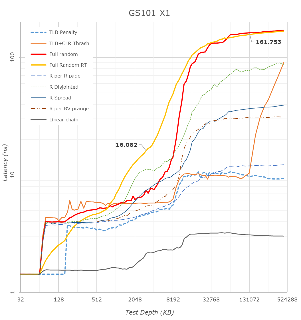
First off, we have to mention that many of the latency patterns here are still quite a broken due to the new Arm temporal prefetchers that were introduced with the Cortex-X1 and A78 series CPUs – please just pay attention to the orange “Full Random RT” curve which bypasses these.
There’s a couple of things to see here, let’s start at the CPU side, where we see the X1 cores of the Tensor chip being configured with 1MB of L2, which comes in contrast with the smaller 512KB of the Exynos 2100, but in line with what we see on the Snapdragon 888.
The second thing to note, is that it looks like the Tensor’s DRAM latency isn’t good, and showcases a considerable regression compared to the Exynos 2100, which in turn was quite worse off than the Snapdragon 888. While the measurements are correct in what they’re measuring, the problem is a bit more complex in the way that Google is operating the memory controllers on the Google Tensor. For the CPUs, Google is tying the MCs and DRAM speed based on performance counters of the CPUs and the actual workload IPC as well as memory stall % of the cores, which is different to the way Samsung runs things which are more transactional utilisation rate of the memory controllers. I’m not sure of the high memory latency figures of the CPUs are caused by this, or rather by simply having a higher latency fabric within the SoC as I wasn’t able to confirm the runtime operational frequencies of the memory during the tests on this unrooted device. However, it’s a topic which we’ll see brought up a few more times in the next few pages, especially on the CPU performance evaluation of things.
The Cortex-A76 view of things looks more normal in terms of latencies as things don’t get impacted by the temporal prefetchers, still, the latencies here are significantly higher than on competitor SoCs, on all patterns.
What I found weird, was that the L3 latencies of the Tensor SoC also look to be quite high, above that of the Exynos 2100 and Snapdragon 888 by quite a noticeable margin. I noted that one weird thing about the Tensor SoC, is that Google didn’t give the DSU and the L3 cache of the CPU cluster a dedicated clock plane, rather tying it to the frequency of the Cortex-A55 cores. The odd thing here is that, even if the X1 or A76 cores are under full load, the A55 cores as well as the L3 are still running at lower frequencies. The same scenario on the Exynos or Snapdragon chip would raise the frequency of the L3. This behaviour and aspect of the chip can be confirmed by running at dummy load on the Cortex-A55 cores in order to drive the L3 higher, which improves the figures on both the X1 and A76 cores.
The system level cache is visible in the latency hump starting at around 11-13MB (1MB L2 + 4MB L3 + 8MB SLC). I’m not showing it in the graphs here, but memory bandwidth on normal accesses on the Google chip is also slower than on the Exynos, but I think I do see more fabric bandwidth when doing things such as modifying individual cache lines – one of the reasons I think the SLC architecture is different than what’s on the Exynos 2100.
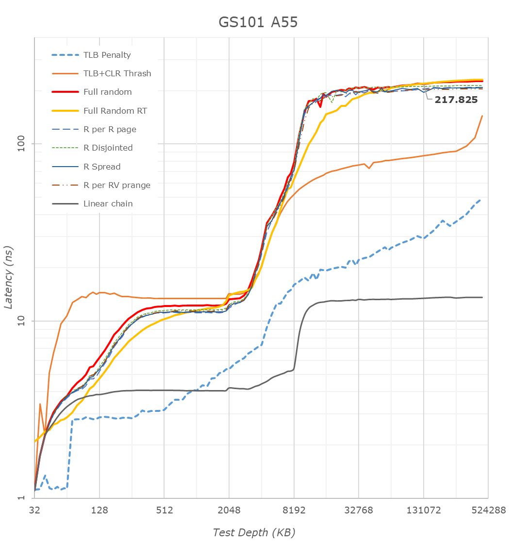
The A55 cores on the Google Tensor have 128KB of L2 cache. What’s interesting here is that because the L3 is on the same clock plane as the Cortex-A55 cores, and it runs at the same higher frequencies, is that the Tensor’s A55s have the lowest L3 latencies of the all the SoCs, as they do without an asynchronous clock bridge between the blocks. Like on the Exynos, there’s some sort of increase at 2MB, something we don’t see on the Snapdragon 888, and I think is related to how the L3 is implemented on the chips.
Overall, the Tensor SoC is quite different here in how it’s operated, and there’s some key behaviours that we’ll have to keep in mind for the performance evaluation part.


108 Comments
View All Comments
anonym - Sunday, November 7, 2021 - link
I don't have any data but A76 is more efficient than A78 while relatively lower performance region. According to following DVFS carves, A77 is out of the question.https://images.anandtech.com/doci/15813/A78-X1-cro...
boozed - Tuesday, November 2, 2021 - link
So do we call this design "semi-custom" or "very-slightly-custom"?watzupken - Wednesday, November 3, 2021 - link
I think we have come to a point that pushing performance for mobile devices is starting to slow down big time, or in some cases like Exynos where we see regressions. The SOC gets refreshed each year, pushing for higher performance. The fabs however is slower to catch up, and despite the marketing of 7nm, 5nm, 3nm, etc, they may not be anywhere near what is being marketed. In this case, squeezing a fat GPU sounds great on paper, but in real life, the sustained performance is not going to make a huge difference because of the power and heat. In any case, I feel the push for an annual SOC upgrade should slow down because I certainly don't see significant difference in real life performance. We generally only know that last years SOCs are slower only when running benchmarks. Even in games, last gen high end SOCs can still handle challenging titles. Instead, they should focus on making the SOCs more power efficient.damianrobertjones - Wednesday, November 3, 2021 - link
All I want is for all phones to be able to record the front and rear camera at the same time. VLog fun. Such a simple thing... .Whiteknight2020 - Wednesday, November 3, 2021 - link
Not India, China, UK, Russia, most of the EU, Africa. Which is the vast majority of the world's population and the vast majority of the world's phones, a great many of which are still feature phones.Whiteknight2020 - Wednesday, November 3, 2021 - link
Not India, China, UK, Russia, most of the EU, Africa. Which is the vast majority of the world's population and the vast majority of the world's phones, a great many of which are still feature phones.eastcoast_pete - Wednesday, November 3, 2021 - link
To me, one of the most interesting points about this "meh" first Google custom SoC is that it was created with lots of Lego blocks from Samsung; I guess Google working with Qualcomm was either out of the question or not something either was willing to do. Maybe this was about Google wanting to show QC that they can develop a Pixel smartphone without them, maybe the two compete too closely on ML/AI, or maybe they just don't like each other much right now - who knows? Still, an SD 888-derived SoC with Google TPU would have likely been better on performance and efficiency. This one here is an odd duck. As for the Pixel 6, especially the Pro: camera is supposed to be spectacular, but with the battery life as it is and, of course (Google, after all), no expandable storage and no 3.5 mm headphone connectors, it missed the mark for me. But, the Pixels are sold out, so why would Google change?Whiteknight2020 - Wednesday, November 3, 2021 - link
If you want a "really excellent camera", sorry to disappoint you but you'll need to be buying an actual camera. The only thing a multipurpose portable computing device can ever be excellent at is being a multipurpose portable computing device.FunBunny2 - Wednesday, November 3, 2021 - link
"a multipurpose portable computing device."isn't that pretty much verbatim what Stevie said when he showed the original iPhone? nothing has really changed since. it was, kinda, a big deal when Stevie intoned that the thingee incorporated 3, count em 3!, devices that you had to carry that day!!! internet, phone, and number 3 (whatever that was). is a 2021 smartphone really anything more?? I mean, beyond the capacity of more transistors. thank ASML (and some really smart physicists and engineers) for that not Apple or Samsung or Google or ... last time I checked Apple's 'our own ARM' SoC is just bigger and wider ARM ISA, due to the, so far, increasing transistor budget available at the foundries.
that all begs the fundamental question: if Apple and The Seven Dwarfs have access to the same physical capital (ASML, et al) why the difference? if everybody spends time and money tweaking a function (that they all need, one way or another), in some time (short, I'll assert) The One Best Way emerges. the task, in the final analysis, is just maths. of course, Best is not a point estimate, as many comments make clear; there're trade offs all along the line.
it would be fun to use one of the Damn Gummint's supercomputers (weather or nucular bomb design) to spec a SoC. wonder how different the result would be?
NaturalViolence - Wednesday, November 3, 2021 - link
The math for the memory bandwidth doesn't check out. From the article:"4x 16-bit CH
@ 3200MHz LPDDR5 / 51.2GB/s"
But 3200MHz x 64 bit is 25.6GB/s, not 51.2GB/s. So which is it?