TSMC: N2 To Start With Just GAAFETs, Add Backside Power Delivery Later
by Anton Shilov on June 29, 2022 12:00 PM EST- Posted in
- Semiconductors
- TSMC
- GAAFET
- 2nm
- N2
When TSMC initially introduced its N2 (2 nm class) process technology earlier this month, the company outlined how the new node would be built on the back of two new cutting-edge fab techniques: gate-all-around transistors, and backside power rails. But, as we've since learned from last week's EU symposium, TSMC's plans are a bit more nuanced than first announced. Unlike some of their rivals, TSMC will not be implementing both technologies in the initial version of their N2 node. Instead, the first iteration of N2 will only be implementing gate-all-around transistors, with backside power delivery to come with a later version of the node.
So far, TSMC has mentioned two distinctive features of N2: nano sheet gate-all-around (GAA) transistors, and backside power rails. GAA transistors have two unique advantages over FinFETs: they solve many challenges associated with the leakage current since GAAFET's channels are horizontal and are surrounded by gates around all four sides. Meanwhile, backside power rail enabled improved power delivery to transistors, which increases performance and lowers power consumption.
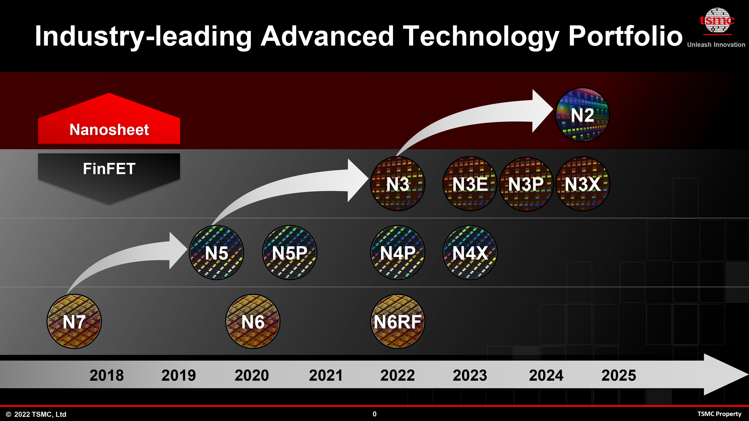
But, as it turns out, TSMC is not planning to start with both nanosheet GAA transistors and backside power rails in the initial generation of its N2 process technology. As disclosed by the company last week at their EU symposium, the first generation of N2 will only feature gate-all-around transistors. Backside power delivery, on the other hand, will come later with more advanced implementations of N2.
At this point the company hasn't said too much as to why they're not rolling out backside power delivery as part of their initial N2 node. But, in discussing the bifurcation, TSMC has noted that backside power delivery will ultimately add additional process steps, which the company is seemingly looking to avoid on their first try with GAAFETs.
The lack of backside power delivery in the original version of the N2 fabrication technology perhaps explains rather moderate performance improvement of N2 when compared to N3E node. While for high-performance computing (CPUs, accelerators, etc.) a 10% to 15% performance improvement at the same power and complexity does not seem to be impressive, a 25% to 30% power drop at the same speed and complexity seems to be very good for mobile applications.
| Advertised PPA Improvements of New Process Technologies Data announced during conference calls, events, press briefings and press releases |
|||||
| TSMC | |||||
| N5 vs N7 |
N3 vs N5 |
N3E vs N5 |
N2 vs N3E |
||
| Power | -30% | -25-30% | -34% | -25-30% | |
| Performance | +15% | +10-15% | +18% | +10-15% | |
| Chip Density* | ? | ? | ~1.3X | >1.1X | |
| Volume Manufacturing |
Q2 2022 | H2 2022 | Q2/Q3 2023 | H2 2025 | |
*Chip density published by TSMC reflects 'mixed' chip density consisting of 50% logic, 30% SRAM, and 20% analog.
Considering that TSMC always offers multiple versions of its nodes, that TSMC has several variants planned for N2 is not all that surprising. Nonetheless, it is a bit odd to see that TSMC is taking a rather long road to backside power delivery.
Compared and contrasted to the competition, this will end up being a notable difference from how rival Intel is planning to handle their own GAAFET/backside power transition with the Intel 20A process. Intel intends to introduce its GAA RibbonFET transistors and PowerVia interconnects together in mid-2024 – going so far as to create an internal pseudo node just to focus on RibbonFET development. TSMC, on the other hand, is taking a more cautious approach to risks and innovations, one which potentially has TSMC moving at a slower pace, but is also an approach that has traditionally been a better fit for TSMC's need to deliver more constant and consistent updates to its fab offerings.
And while we're still a few years out, it will be interesting to see what this means for the competitiveness of TSMC's first-generation N2 node. Will a GAAFET process without backside power delivery be at a meaningful disadvantage? Per current schedules, we'll find out the answer to that in the second half of 2025, when TSMC's first N2 node is slated to enter high-volume manufacturing (HVM).


14 Comments
View All Comments
Vitor - Wednesday, June 29, 2022 - link
So it really seems silicon progress will be at a dead end by 2035, right? After N2 thinks will get so tiny and tricky that only a new material will be able to provide substantial improvements.Khanan - Wednesday, June 29, 2022 - link
Tech advancement will never stop, could be that it slows down but it’ll never stop.DougMcC - Wednesday, June 29, 2022 - link
Meh. It will be challenging to get more dense than Hydrogen fabrication at 31pm, in a 3d layered gas I guess? We're rapidly closing in on the fundamental constraints of the universe we live in.nandnandnand - Wednesday, June 29, 2022 - link
They could do tiny node steps into the late 2030s, or move to a roadmap that emphasizes 3D stacking improvements like what was done with V-NAND.