Google's Tensor inside of Pixel 6, Pixel 6 Pro: A Look into Performance & Efficiency
by Andrei Frumusanu on November 2, 2021 8:00 AM EST- Posted in
- Mobile
- Smartphones
- SoCs
- Pixel 6
- Pixel 6 Pro
- Google Tensor
GPU Performance & Power
The Google Tensors GPU is quite a beast. A Mali G78 with 20 cores, it’s sporting 42% more cores than the Exynos 2100 implementation, and only comes second after HiSilicon’s Kirin 9000. However, unlike the more power efficient N5 process node of the Kirin 9000, the Tensor SoC comes on the same process node as on the Exynos 2100. Having a much larger GPU, one would expect Google to drive the block at lower frequencies, in order to achieve better energy efficiency. To our surprise, the G78MP20 runs at up to 1GHz on the tiler and L2, and up to 848MHz on the shader cores, which is essentially the same as the smaller Exynos 2100 implementation of the GPU. Of course this immediately raises red flags for the Tensor when it comes to power consumption, as the chip certainly can’t pull out a rabbit out of a hat in terms of efficiency, so let’s see what happens:
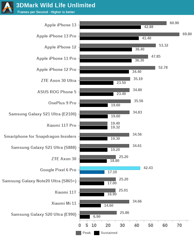
In 3DMark Wild Life unlimited, the first thing to note is that for some reason the regular Pixel 6 didn’t want to run the test as it errored out due to memory – I’m not sure what happened here, but it was isolated to the baseline model as the Pro unit had no issues.
The Pixel 6 Pro’s peak performance is respectable, however it’s only 21% faster than the Exynos 2100, not exactly what we’d expect from 21% more cores. A large issue with Mali GPUs of late has been that while you can throw more shader cores at the issue, the shared resources such as the tiler and L2 still remain as a single unit on the GPU. The G78’s ability to clock this part of the GPU higher is taken advantage of by Google in the Tensor implementation of the GPU, however that’s only 16% faster in pure clock frequency – maybe the workload is bottlenecked somewhere in this part of the GPU architecture.
Sustained performance off the start doesn’t look too good for the Pixel 6 Pro as it throttles considerably once the device gets hot, more on this in a bit.
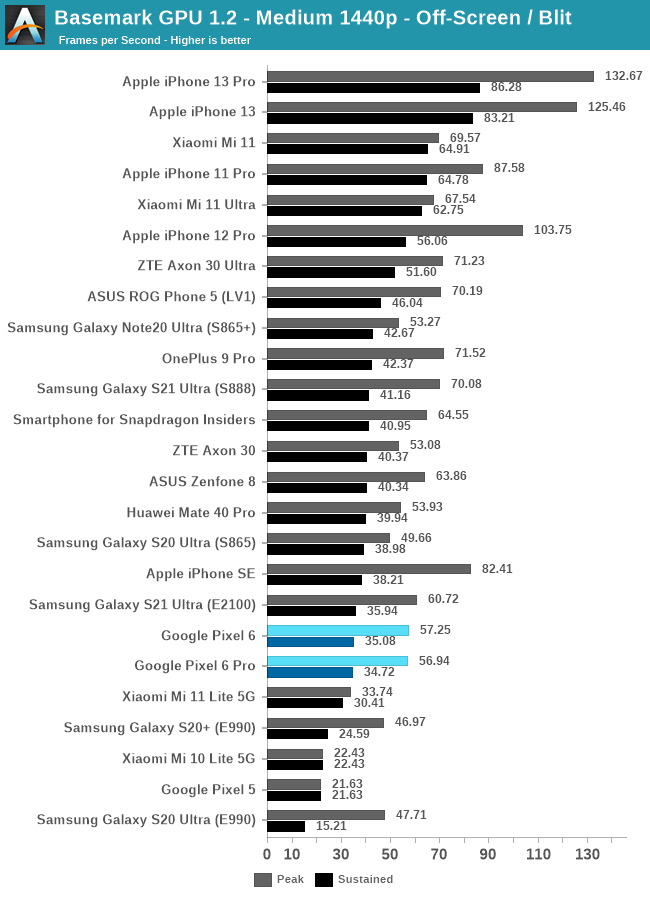
In Basemark GPU, the Pixel 6 phones both showcase odd peak performance figures that are way lower than we expected, here the chip doesn’t even manage to outperform the Exynos 2100. I’m not sure what the technical explanation here is, as on paper, the chip should be faster.
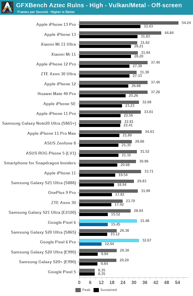
In Aztec High, the peak performance of the Tensor is again below what you’d expect, at +14% vs the Exynos 2100, and slightly ahead of the Snapdragon 888.
Sustained performance is quite bad here, and especially the Pixel 6 Pro seems to be running more severe throttling than the Pixel 6.
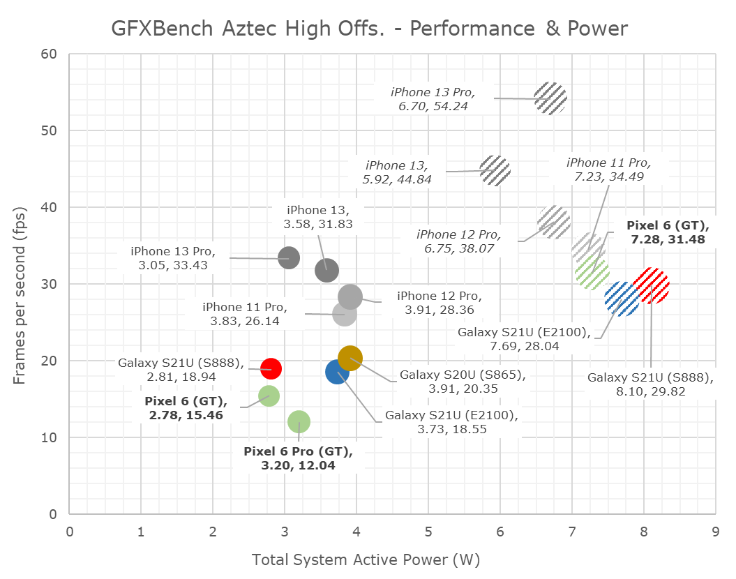
Looking at the power consumption of the phones, at peak performance, the Pixel 6 lands in around 7.28W, however this figure is a bit misleading. In actuality, the phone is running peak power figures in excess of 9-10W, but this is so much power, that the SoC isn’t able to complete a single run of the benchmark without throttling, so average power for a given run is actually much lower. This would also explain as to why our peak performance figures are less than what’s expected of a GPU clocked this high, it simply can’t maintain that speed for long enough to give off an FPS figure at the peak frequencies.
At sustained frequencies, the Pixel 6 and Pixel 6 Pro end up with different spots, however both are at quite low power figures around 3W.
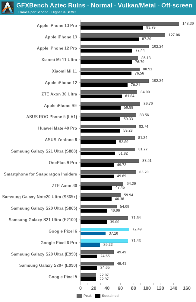
Aztec normal shows similar results, peak performance of the GPU is barely any better than the smaller configuration Exynos 2100 unit, and sustained performance figures are also significantly lower.
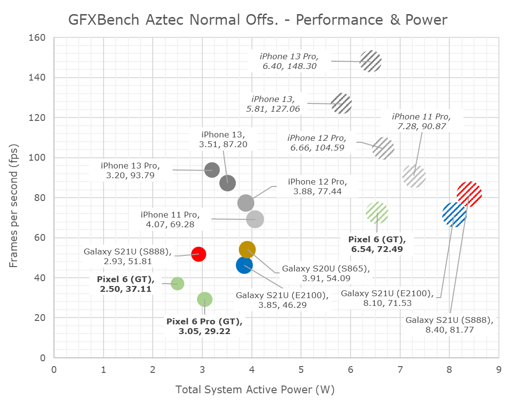
Sustained power after throttling on the phones is also quite weird here, as the phone seemingly throttles to <3W on the SoC. The Pixel 6 for some reason appears to have better power characteristics, it’s possible that chip bin has lower power than my 6 Pro unit.
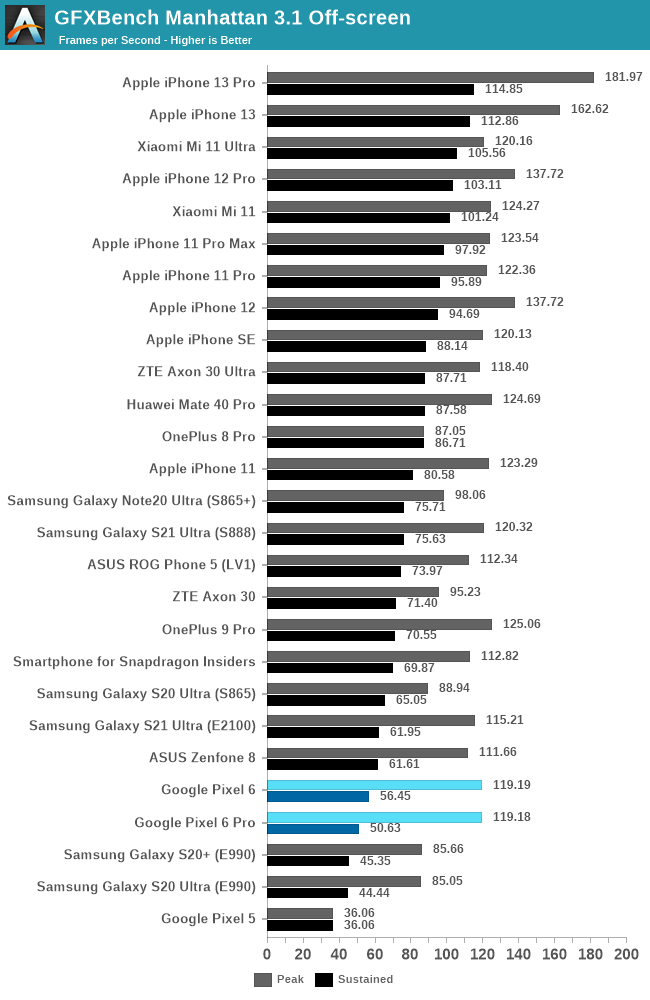
Manhattan 3.1 shows a similar peak and sustained performance standing, which isn’t too favourable for the Tensor.
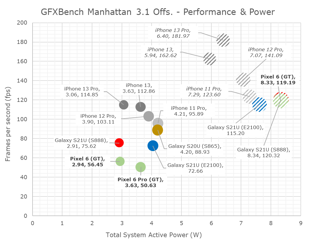
Power levels in Manhattan are higher than the Aztec benchmarks, I think the CPUs, or the DRAM contribute to more of the power due to the higher achieved framerates, and it slightly helps the heat dissipation rather than having everything focused on the GPU.
Overall, the GPU performance of the Google Tensor is quite disappointing. On paper, the massive G78MP20 GPU seemed like a juggernaut at the frequencies Google delivers the chip in, but in practice, it doesn’t reach the theoretical levels of performance. That being said, over the last year of SoC releases, almost every vendor in the industry has introduced some absurd ultra-high-power GPU configuration that throttles quickly. Why they do this, I don’t know, GPU compute for burst performance is always one of the reasons given, so maybe Google is also aiming the GPU towards compute rather than gaming.
In terms of sustained performance levels, the larger GPU in theory should have allowed it to run at lower frequencies, thus at better efficiency, and in turn deliver more performance than a smaller implementation like that of the Exynos 2100. The reality here is that the Pixel 6 phones struggle with thermal dissipation, and it’s something that seems to be completely unrelated to the chip itself.
Source: PBKreviews
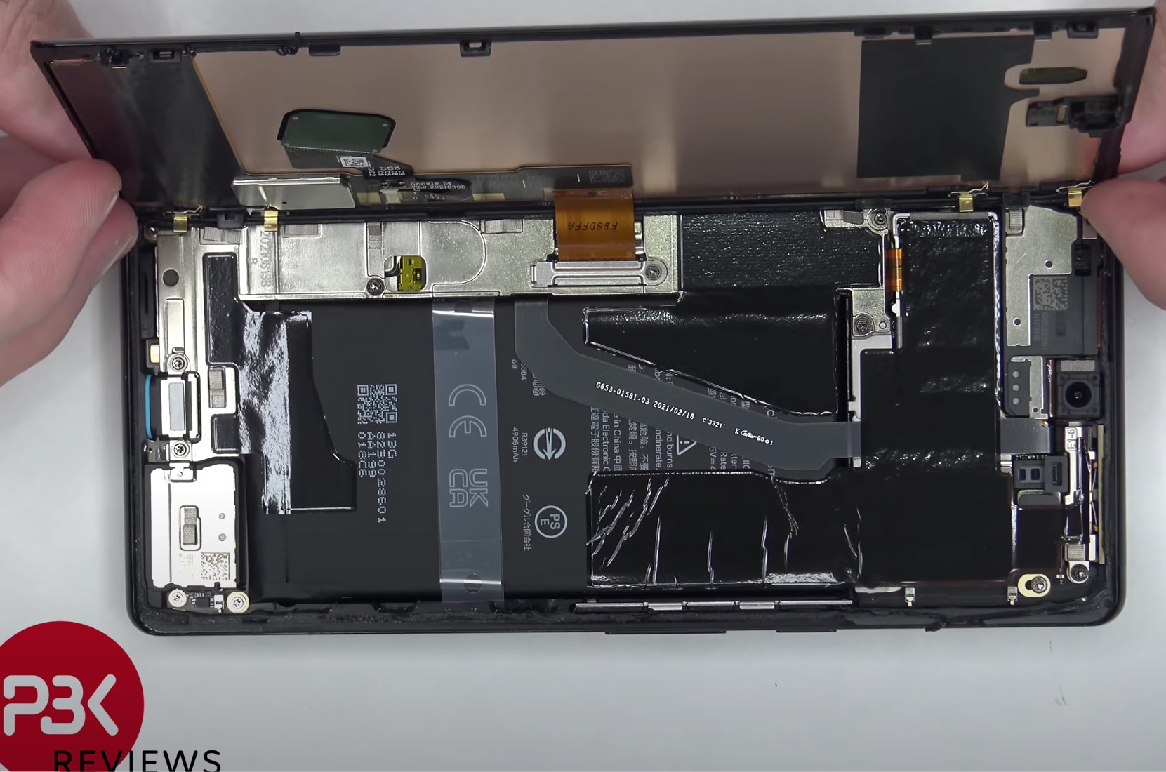
Both the Pixel 6 and Pixel 6 Pro are quite special in their hardware designs, in that they’re one of the rare Android devices out there which adopt an internal hardware design which doesn’t have a midframe adhered to the display panel. Looking at various teardowns of the phone, we can see that the display is relatively easily removable from the rest of the phone body, a design that’s actually more similar to Apple’s iPhones than any other Android flagship. This bodes well for the repairability of the screen, but it doesn’t do well for the thermal dissipation of the SoC. Much like iPhones have issues with thermal dissipation, and having much lower sustained power levels under stress, the Pixel 6 phones also suffer from the same issue as they cannot effectively use the display panel as a heat sink. This comes in contrast with other flagship Android devices – the Galaxy S21 Ultra for example has its display panel adhered to the midframe of the phone, it's not great for repairability, but it allows Samsung to employ a gigantic thermal dissipation pad the size of half of the phone footprint, with a direct heat pathway from the SoC to the display. Other thermally optimised devices out there share similar designs, able to better dump heat onto the full body of the phone.
The Pixel 6 Pro in contrast, has quite stark heat spots, with the left side of the phone, near the SoC, getting quite hot at up to 45°C, but at the same time the right side of the device here barely reaches 30-33°C, which is a large temperature gradient and signifies bad heat transfer abilities. Also, while I’m not sure how other people feel about this, but it does make the Pixel 6 phones feel more “hollow” in their build quality, but that might just be a nit-pick.
In any case, the Google Tensor’s chip gaming performance might be adequate, it’s no better than the Exynos 2100, and it gets further handicapped by the thermal design of the Pixel 6 phones. Generally, one can say it’s not the best phone for high-end gaming, which lines up with the subjective experiences with the devices in actual gaming demanding games like Genshin Impact.


108 Comments
View All Comments
jaju123 - Tuesday, November 2, 2021 - link
Thanks Andrei, using the P6 Pro right now and it is remarkably smooth in terms of general UI regardless of the benchmark scores etc., in comparison to other phones. I suspect the scheduling and UI rendering side of things are contributing here. Very much looking forward to the camera review!jiffylube1024 - Wednesday, November 3, 2021 - link
Same experience here on a P6 regular.I went from an S20 (regular) to the P6 pro. Wife has the S21 regular.
My experience so far:
UI is insanely fast and smooth on the P6. Everything is buttery smooth, no lag ever. It's a joy to use. The S20 is a very fast phone, but it did have the very occasional hiccup when switching between many different apps. So far, this hasn't happened on the Pixel 6 at all.
The S20 had nicer hardware overall, and the hand size was perfect. S20 screen gets a bit brighter, was a tiny bit sharper, and auto-adjust brightness was basically perfect on the S20, it's a little bit imperfect on the P6 (occasionally goes up or down in low light for no reason).
All in all, I'm very happy with the Pixel 6. If the Pixel 7 comes in a 6"-6.2" version next year, I may have to switch again, though!
Kangal - Wednesday, November 3, 2021 - link
That's because it is running a mostly Stock OS. Google severely limits background tasks when in use, and prioritises touch input... as opposed to say Samsung, which starts off slower and raises frequency in steps, whilst continuing background tasks. This slows the experience, but can boost efficiency, depending on the user.Now, the Cortex-A76 is actually not bad. It's a great chip, as it's quiet fast while being efficient. It requires less area and density compared to the A77 and A78. So Google didn't make a mistake here. By going for the A76, they were able to upgrade to have two Cortex-X1 cores. It is a design choice. Another design choice could be 3x X1 and 5x A55, cutting out the Middle-cores for a more simpler design. Or you could potentially have 4x A78 and 4x A55, and have the A78 cores clock higher, for better sustained performance than X1. These are all different design choices, one can be better than another, but it depends on the circumstances.
Kangal - Wednesday, November 3, 2021 - link
I just want to add my viewpoint on the performance and efficiency of this chipset/phone.AI/ML/NPU/TPU Benchmark: GeekBench ML 0.5
This looks like the most accurate representation. The iPhone 13 has an impressive AI performance because their SDK is better fleshed out, their software is coded more natively, and the SoC has pretty impressive specs Cache, CPU, GPU to help with such tasks. The GS101 wins in the Android ecosystem by a wide margin, followed by QSD 888, MediaTek Dimensity, then lastly Exynos. We can see the proper AI chart here: https://images.anandtech.com/graphs/graph17032/126...
GPU Benchmark: GFxBench Aztec Ruins High (Sustained)
This looks like the most accurate representation. Again Apple flexes its lead with its optimised software and cutting-edge hardware. Larger phones with better cooling manage to score higher, and giving preference to Qualcomm's mature drivers, followed by Huawei's node advantage, then the mediocre attempts by Exynos which is tied for the last spot with the GS101. We can see the proper GPU chart here: https://images.anandtech.com/graphs/graph17032/101...
CPU Multithread Benchmark: GeekBench 5 (crude Single/Multithread)
In the multi-thread test, it shows how sacrificing the middle cores has affected the total score, where it helps to boost the performance of the first 1-2 threads. So at least that design choice is captured. We can see the proper Multithread CPU chart here: https://images.anandtech.com/graphs/graph16983/116...
CPU Single-core Benchmark: SPEC 2017 (fp scores)
The SPEC test is more nuanced. We've established that Anandtech has made huge blunders here. Instead of reporting the Power Draw (watts) of the chipset, they instead try to calculate Energy Consumed (joules) by estimating it crudely. It is for that reason, we get some very inconsistent and wrong data. Such as Apple's Efficiency cores using less power than a Cortex-A53, yet producing scores in line with the Cortex-A78.
So instead, we will focus on the fp-scores instead of the int-scores, since this actually scales better from chipset to chipset. And we will focus on the Power Draw figures, to get the proper data. In particular, the tests of 526, 544, and 511 are quite revealing. We can see the proper CPU chart here:
https://images.anandtech.com/doci/16983/SPECfp-pow...
As a summary of the raw data, here:
Chipset-CoreType: Performance Value / Watts Recorded = Efficiency Score
Apple A14-E: 2.54 / 0.42 = 6.05
Apple A15-E: 3.03 / 0.52 = 5.83
Dim 1200-A55: 0.71 / 0.22 = 3.23
QSD 888-A55: 0.85 / 0.30 = 2.83
Exy 990-A55: 0.84 / 0.50 = 1.68 (? too low! Watts probably not recorded correctly)
Exy 2100-A55: 0.94 / 0.57 = 1.65 (? too low! Watts probably not recorded correctly)
GS 101-A55: 0.88 / 0.59 = 1.49 (? too low! Watts probably not recorded correctly)
Apple A15-P: 10.15 / 4.77 = 2.13
QSD 870-A77: 5.76 / 2.77 = 2.08
Apple A14-P: 8.95 / 4.72 = 1.90
QSD 888-X1: 6.28 / 3.48 = 1.80
GS 101-X1: 6.17 / 3.51 = 1.76
Dim 1200-A78: 4.71 / 2.94 = 1.60
Exy 2100-X1: 6.23 / 3.97 = 1.57
Exy 990-M5: 4.87 / 3.92 = 1.24
Andrei Frumusanu - Thursday, November 4, 2021 - link
> We've established that Anandtech has made huge blunders here. Instead of reporting the Power Draw (watts) of the chipset, they instead try to calculate Energy Consumed (joules) by estimating it crudely.I have no idea what you're referring to. The power draw is reported right there, and the energy isn't estimated, it's measured precisely. The A55 data is correct.
Perf/W is directly inversely relative to energy consumption if you would actually plot your data.
Kangal - Saturday, November 6, 2021 - link
The Specific Power Draw makes sense in the context of these comparisons. For the longest time in this industry, they've always talked about Performance per Watt. No-one, not even Intel (and they've been know to be quite shady) uses Performance per Joules.The total energy consumed in Joules is simply irrational. One can then make a flawed comparison of how much processing could be made through the consumption of a cupcake if you read it's nutritional content. Not only that, if you actually look at the data you guys submitted, it has a lot more variance with Joules, whilst Watts shows a lot more consistent results. Your energy consumed is an estimate, not what is specifically used by the cores when running.
For instance, when using Joules, it makes Apple's Efficiency cores seem to use slightly less power than a Cortex-A55, whilst performing benchmarks slightly faster than a Cortex-A76. If that is true, then no Android phones would be sold above $500 as everyone would simply buy iPhones. It's like comparing a 2011 processor (48nm Dual Cortex-A9) to a 2015 processor (16nm Octa Cortex-A53), so it's not only using less power, but delivering more than x4 times the performance. Ludicrous. You just cannot magically wave away discrepancies that big (x7.43). On the other hand, if you plot it using Watts, you get a deeper picture. Apple's Efficiency cores use about double the energy as a Cortex-A55 but in turn they deliver four times the performance, so the net difference is a much more palatable x2.14 leap in efficiency (at least in max performance comparison). And I'm comparing the latest Apple (A15) to Android (QSD 888) cores.
If the A55 data is as accurate as you say, why do you have discrepancies there as well?
For example, QSD 888 versus Google Silicon-101... they're both using off-the-shelf Cortex-A55. Yet, the Qualcomm's chipset is apparently drawing only 0.30 Watts, compared to 0.59 Watts... which is about x2 less. And both perform fairly close scores at 0.85 versus 0.88, making their total efficiency difference of x1.90 (2.83 vs 1.49) puzzling. So something is a miss. Going off the Joules Estimates doesn't fix the issue either, as you still have an unaccounted x1.83 difference in efficiency still.
With all your resources, you guys never got curious about such discrepancies?
(sorry for being a little obtuse)
dotjaz - Sunday, November 7, 2021 - link
You are obviously uneducated, and don't know what "off-the-shelf" means in any chips. Physical implementation varies a lot even on the same process with the same IP. Either you or Cadence are lying. I'd rather believe a reputable company with decades of experience.https://www.anandtech.com/show/16836/cadence-cereb...
Kangal - Sunday, November 7, 2021 - link
Snapdragon 888: 4x Cortex-A55 @ 1.80GHz 4x128KB pL2, with 4MB sL3, on Samsung5nm (5LPE)
Google Tensor: 4x Cortex-A55 @ 1.80GHz 4x128KB pL2, with 4MB sL3, on Samsung
5nm (5LPE)
Both of these SoC's are using Cortex-A55 cores which were licensed from ARM directly. They are off-the-shelf. These are not custom cores, such as the Mongoose, Early-Kyro, Krait, Denver, Carmel, or the 8-or-so different custom designs released by Apple. If you say that I am lying, then you are also saying that both Google, Qualcomm, are also lying. And note, that they are virtually identical in their specifications and build.
I think you entirely mis-understood the point of Cadence is about. Sure, even on the same chips there are variance, the so-called "silicon lottery". But be realistic, how much of a difference do you think it is? I'll give a hint, the larger the silicon, the more the variance, and the bigger the difference. If you check the latest data from the now bankrupt siliconlottery.com service, the difference with the 3950X is (worst) 4.00Ghz versus 4.15Ghz (best). At best that is a 3-point-something-percent difference, so let's say it is 5%... and this difference is likely to be less on smaller chips. But even if we accept 5%, that is nowhere near x2 variance.
Also, you would be calling AnandTech liars as well:
" the new Cortex-A77 picks up where the Cortex-A76 left off and follows Arm’s projected trajectory of delivering a continued SOLID PERFORMANCE UPLIFT of 20-25% CAGR "...
How is it that we are able to be impressed by a +20% uplift, yet, we completely disregard a +90% difference? It is not logical, and doesn't pass the sniff test. You can call me uneducated all you like, I'm trying to arrive at the truth, since there are big discrepancies with the data provided that I've pointed out to above. I am open to criticism, as everyone should be.
TellowKrinkle - Tuesday, November 9, 2021 - link
Let's look at some unitsPerformance is units of calculation work divided by time. For our graph, some constant times spec runs per second.
Performance per watt is then some constant times (spec runs) / (seconds * watts)
The joules measurement put up there is specifically joules per spec run. One joule is one watt second, so that number would therefore be (watts * seconds) / (spec runs).
Notice the similarity? Joules is 1/(perf per watt).
Hopefully it's clear from this that the "joules" measurement on that graph *is* there to indicate efficiency, just like a perf/watt measurement would be. The only difference is that in the joules graph, high numbers indicate inefficient processors, while in a perf/watt graph, those would be represented by low numbers.
The0ne - Thursday, November 4, 2021 - link
Pixel 4A updated last night to 12 and it runs even smoother. The UI tricks they have done does appear to make a visual difference. So far I'm impressed with 12 aside from the gigantic texts and bars here and there.