TSMC Details 3nm Evolution: N3E On Schedule, N3P and N3X To Deliver 5% Performance Gains
by Anton Shilov on April 26, 2023 5:15 PM EST
Alongside some new announcements for their 2nm process node plans, TSMC has also released a progress and roadmap update for their N3 family process technologies at today's 2023 North American Technology Symposium. TSMC's final generation of FinFET-based process nodes, the N3 family is expected to remain around in some shape or form for many years to come as the densest node available for customers who don't need a more cutting-edge GAAFET-based process.
TSMC's big roadmap updates on the N3 front were with N3P and its high performance variant, N3X. As revealed today by TSMC, N3P will be an optical shrink of N3E, offering enhanced performance, reduced power consumption, and increased transistor density compared to N3E, all while maintaining compatibility with N3E's design rules. Meanwhile, N3X will wed extreme performance with 3nm-class densities, offering higher clockspeeds for high performance CPUs and other processors.
N3E: 3nm for Everyone Is on Schedule
As a quick refresher, TSMC's N3 (3nm-class) family of process technologies is comprised of several variants, including baseline N3 (aka N3B), relaxed N3E with reduced costs, N3P with enhanced performance and chip density, and N3X with higher voltage tolerances. Last year the company also talked about N3S with maximized transistor density, but this year the company remains tight lipped about this node and it is not mentioned anywhere in its slides.
TSMC's vanilla N3 node features up to 25 EUV layers (according to China Renaissance and SemiAnalysis), with TSMC using EUV double-patterning on some of them to make for higher logic and SRAM transistor density than N5. EUV steps are expensive in general, and EUV double patterning drives those costs up further, which is why this fabrication process is only expected to be used by a handful of customers who are not as concerned about the high outlay required.
| Advertised PPA Improvements of New Process Technologies Data announced during conference calls, events, press briefings and press releases |
|||
| TSMC | |||
| N3 vs N5 |
N3E vs N5 |
||
| Power | -25-30% | -32% | |
| Performance | +10-15% | +18% | |
| Logic Area Reduction* % Logic Density* |
0.58x -42% 1.7x |
0.625x -37.5% 1.6x |
|
| SRAM Cell Size | 0.0199µm² (-5% vs N5) | 0.021µm² (same as N5) | |
| Volume Manufacturing |
Late 2022 | H2 2023 | |
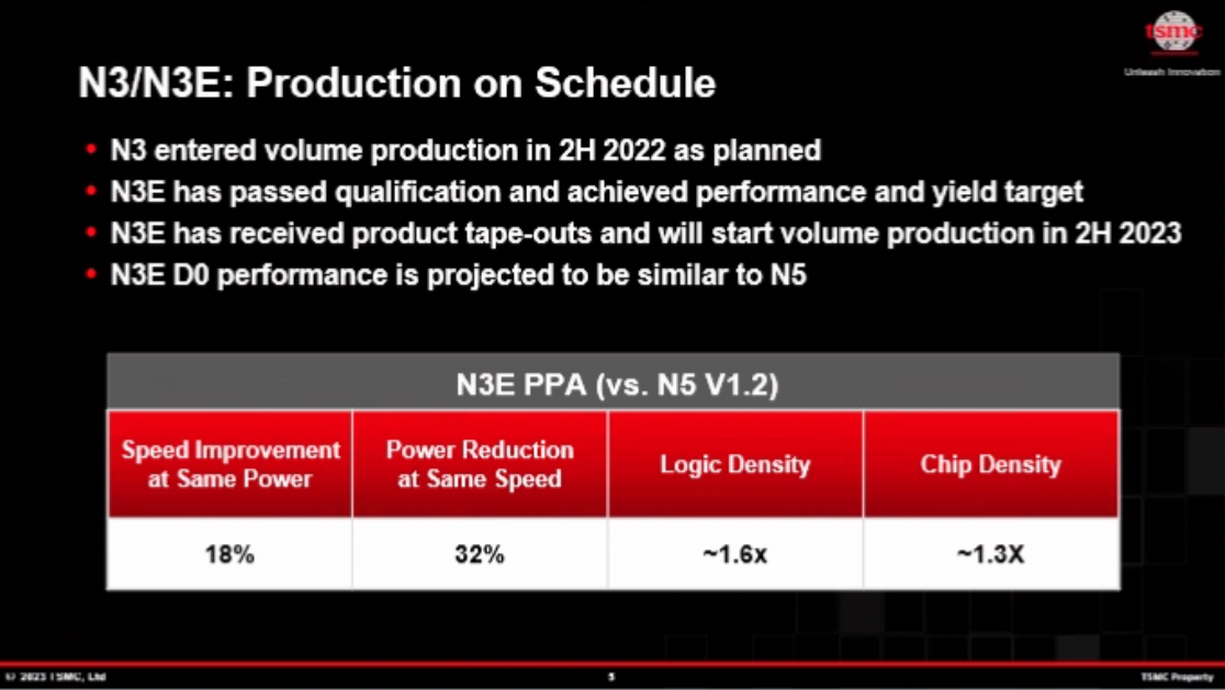
The majority of TSMC's clients interested in a 3nm-class process are expected to use the relaxed N3E node, which according to TSMC is on schedule and achieving their performance targets. N3E uses up to 19 EUV layers and does not rely on EUV double patterning at all (according to data from China Renaissance and SemiAnalysis), reducing its complexity and costs. The trade-off is that N3E offers lower logic density than N3, and it has the same SRAM cell size as TSMC's N5 node, making it somewhat less attractive to those customers who are driving for density/area gains. Overall, N3E promises a wider process window and better yields, which are two crucial metrics in chip fabrication.
"N3E will be better than N3 in terms of yield, process complexity, which directly translating into [wider] process window," said Kevin Zhang, Vice President of Business Development at TSMC.
N3P: Higher Performance, Higher Transistor Density
Following N3E, TSMC will continue to optimize the N3 family's transistor density with N3P, which will build on N3E by offering improved transistor characteristics. The refined process node will allow chip designers to either increase performance by 5% at the same leakage or reduce power by 5% ~ 10% at the same clocks. The new node will also increase transistor density by 4% for a 'mixed' chip design, which TSMC defines as a chip consisting of 50% logic, 30% SRAM, and 20% analog circuits.
As part of their discussion on N3P, TSMC stressed that the density improvement was achieved by adjusting the optical performance of its scanners. So it is likely that TSMC will be able to shrink all types of chip structures here, which will make N3P an attractive node for SRAM-intensive designs.
"N3P is a performance boost, it has a 5% higher performance, at least a 5% higher than N3E," explained Zhang. It also has the 2% optical shrink, which bring transistor density to 1.04x."
| Advertised PPA Improvements of New Process Technologies Data announced during conference calls, events, press briefings and press releases |
|||||
| TSMC | |||||
| N3 vs N5 |
N3E vs N5 |
N3P vs N3E |
N3X vs N3P |
||
| Power | -25-30% | -32% | -5% ~ 10% | higher | |
| Performance | +10-15% | +18% | +5% | +5% Fmax @ 1.2V |
|
| Chip Density | ? | ? | 1.04x | same | |
| SRAM Cell Size | 0.0199µm² (-5% vs N5) | 0.021µm² (same as N5) | ? | ? | |
| Volume Manufacturing |
Late 2022 | H2 2023 | H2 2024 | 2025 | |
Since N3P is an optical shrink of N3E, it will preserve N3E's design rules, enabling chip designers to quickly reuse N3E IP on the new node. Consequently, N3P is also projected to be one of TSMC's most popular N3 nodes, so expect IP design houses like Cadence and Synopsys to offer a variety of IP for this process technology, reaping the benefits of forward compatibility with existing N3E in the process. TSMC says that N3P will be production ready in the second half of 2024.
N3X: Maximum Performance and Density
Finally, for developers of high-performance computing applications like CPUs and GPUs, TSMC has for the past few generations been offering its X family of high voltage, performance-focused nodes. As disclosed at last year's event, the N3 family will be getting its own X variant with the aptly named N3X node.
Compared to N3E, N3X is projected to offer at least 5% higher clockspeeds compared to N3P. This is being accomplished by making the node more tolerant of higher voltages, allowing chip designers to crank up the clockspeeds in exchange for higher overall leakage.
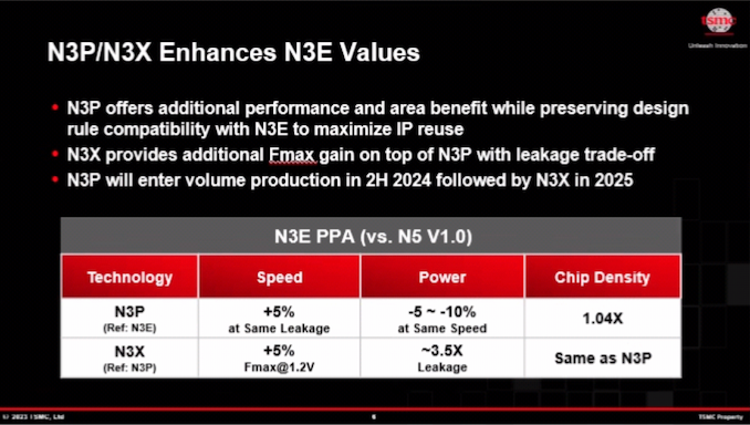
TSMC claims that N3X will support voltages of (at least) 1.2v, which is a fairly extreme voltage for a 3nm-class fabrication process. The leakage cost, in turn, is significant, with TSMC projecting a whopping 250% increase in power leakage over the more balanced N3P node. This underscores why N3X is really only usable for HPC-class processors, and that chip designers will need to take extra care to keep their most powerful (and power-hungry) chips in check.
As for transistor density, N3X will offer the same density as N3P. TSMC has not commented on whether it will also maintain design rule compatibility with N3P and N3E, so it will be interesting to see what ends up happening there.
The final N3 family node in TSMC's current roadmap, the company says that that N3X will be production ready in 2025.
Source: TSMC


13 Comments
View All Comments
Adonisds - Wednesday, April 26, 2023 - link
If N3B started volume manufacturing late 2022 why hasn't wasn't any product announced yet? Are all the N3B production lines idle and bleeding money?Yojimbo - Wednesday, April 26, 2023 - link
I don't think they are idle at this point. They are working overtime but the yields are bad. They were likely idle in 2022, however. Why does TSMC say they started volume manufacturing of N3B in 2022? Because TSMC is always on schedule, even when they are a year late. Firstly, the only reason N3E exists is because the original N3 which they are calling N3B, didn't turn out as intended. As far as I know, only Apple is going to use it, later than they would have wanted, and only for the ultra high end of their product lineup. Rumor has it that TSMC is currently having trouble keeping up with Apple's demand for N3B even for the reduced A17 order. They are producing on it, it's just slow going. Perhaps one could say N3B was around to be available for "volume manufacturing" since late 2022 if one only wanted a small volume and was willing to pay a lot for it. N3B seems like a dead end with N3E set to replace it, supposedly with HVM in H2 2023. TSMC promised N3E HVM would begin 1 year after N3B HVM, and since apparently TSMC always keeps their promises we can't really trust that the H2 2023 situation for N3E will be any better than what the H2 2022 situation for N3B was, even though by now TSMC knows if anyone will actually be producing anything on the supposedly volume-ready node in H2 2023.TeslaDomination - Wednesday, April 26, 2023 - link
I wonder if this year's iPhone will be like the following:iPhone 15, 15 plus, 15 pro, 15 pro plus - A16
iPhone 15 ultra - A17
Adonisds - Thursday, April 27, 2023 - link
What happens while they are still working on yields? Do the use a reduced number of EUV machines and reallocate them to production lines of active nodes or do all the many N3B EUV machines stay idle in the N3B fab?Yojimbo - Friday, April 28, 2023 - link
Just to avoid confusion, I want to stress that they don't directly need less machines because of bad yields. Bad yields means they need more capacity for the same number of good chips. But since Apple most likely originally intended to use N3B for the entire iPhone 15 lineup, they are likely looking at a reduced capacity demand for N3B.But to answer your question, I don't know. My guess would be they didn't have much idle for that long. They never built out the originally intended capacity for N3B because before it became necessary for them to do so they made the necessary decisions with their customers regarding intended usage of the node. TSMC are very good at managing their capacity. In the foundry business that's key to profitability.
TeslaDomination - Wednesday, April 26, 2023 - link
If current rumors are to be believed, Samsung’s 3GAP outperforms N3 and N3E on the latest PDK. The only question now is the yield. I suspect N3E and 3GAP are in the 50% range. 30% for N3.I don’t think TSMC’s domination is a certainty at this moment, and I believe warren buffet’s decision to dump TSMC has less to do with China risks (Why didn’t he sell AAPL if China was a major risk) and more to do with Samsung.
Otritus - Thursday, April 27, 2023 - link
Using the Apple A9 processor and Nvidia Pascal GPUs, we can estimate the performance-per-watt gap between Samsung's 14LPP and TSMC's 16FF+. I estimate the gap between the 2 to be at 1.3-1.35x, so I'll be using 1.32x for my calculations.The 1.32x figure can be demonstrated to be close to reality by comparing Nvidia's Ampere graphics cards to their Turing predecessors. By isolating the GPU core power, adjusting for frequency, and assuming a n% increase in transistors is a n% increase in power and no efficiency improvements from the Ampere architecture alone, we can determine Ampere to be 26.3% more efficient than Turing. Theoretically, 12FF to 8LPP would be a gain in 27.3% in efficiency. The power adjustment for frequency is based on the formula of f^3.33, wherein a 10% increase in frequency results in an increase in power of 37.4%. This is because the formula for dynamic power is power = cfv^2 (f is frequency and v is voltage) and voltage scaling isn't typically linear with frequency, but slightly above it. The f^3.33 is surprisingly accurate with a wide range of processors as long as they aren't falling off a voltage-frequency cliff.
16FF+ -> N7 is a gap of 2.5x, N7 to N5 is a gap of 1.43x, and N5 to N4P is a gap of 1.28x. Altogether, 16FF+ to N4P is a gain of 4.59x efficiency or a reduction in power of 78.16%. 16FF+ to N3 would be 4.76-5.1x efficiency (a decrease in power of 79-80.4%). 16FF+ to N3E would be 5.25x efficiency or a reduction in power of 80.96%.
14LPP -> 10LPE is a gap of 1.43x, 10LPE -> 10LPP is a gap of 1.18x, 10LPP -> 8LPP is a gap of 1.11x, 10LPE -> 7LPP is a gap of 2x (8LPP -> 7LPP would be 1.53x gain), 7LPP -> 5LPE a gap of 1.25x, and 7LPP -> 3GAE a gap of 2x (1.6x gain vs 5LPE). All together 14LPP to 3GAE is a gain of 5.71x efficiency or a reduction in power of 82.5%.
TL;DR: Doing this math means that if 16FF+ is tied with 14LPP (which it is not), then 3GAE would be 8.8% ahead of N3E and 12-20% ahead of N3. Adjusting for the 1.32x difference in efficiency, puts N3E 21.3% ahead and N3 10-17.9% ahead. Samsung historically improves efficiency in their second iteration by about 10-20%, so 3GAP will likely be behind N3E and tied with N3. The rumors of 3GAP are probably wrong based on math, historical progression, and Samsung's failure to make an excellent FinFET node while GAAFETs are even more complex. If GAAFETs or Samsung's engineers turn out to be better than expected, it's possible that 3GAE and thus 3GAP are better than expected and can beat N3 class nodes.
Otritus - Thursday, April 27, 2023 - link
The GPU power isolation came from a friend of mine who analyzed the 3070 and and 2080. Both were minimally cut down variants of the 104 GPU of their generation. Using power virus loads he got 151 watts for the 3070 and 149 watts for the 2080.Otritus - Thursday, April 27, 2023 - link
This figure excludes vrm losses, memory, and other power like fans and lights.Otritus - Thursday, April 27, 2023 - link
My friend was also the one who taught me the f^3.33 formula for estimating power differences from frequency changes. It’s pretty accurate across various GPUs. Unsure if this extends to all nodes when voltage and frequency scale well, or just FinFET nodes from Samsung and TSMC as my friend only demonstrated with FinFET GPUs.