Samsung Kicks Off DDR5 DRAM Production on 12nm Process Tech, DDR5-7200 in the Works
by Anton Shilov on May 18, 2023 7:00 PM EST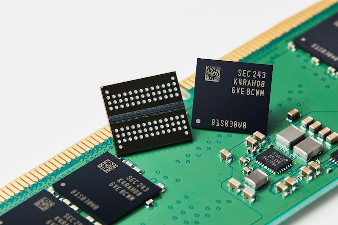
Samsung on Thursday said it had started high volume production DRAM chips on its latest 12nm fabrication process. The new manufacturing node has allowed Samsung to reduce the power consumption of its DRAM devices, as well as decrease their costs significantly compared to its previous-generation node.
According to Samsung's announcement, the company's 12nm fabrication process is being used to produce 16Gbit DDR5 memory chips. And while the company is already producing DDR5 chips with that capacity (e.g. K4RAH086VB-BCQK), the switch to the newer and smaller 12nm process has paid off both in terms of power consumption and die size. As compared to DDR5 dies made on the company's previous-generation node (14nm), the new 12nm dies offer up to 23% lower power consumption, and Samsung is able to produce 20% more dies per wafer (i.e., the DDR5 dies are tangibly smaller).
Samsung says that the key innovation of its 12nm DRAM fabrication process is usage of new high-k material for DRAM cell capacitors that enabled it to increase cell's capacitance to boost performance, but without increasing their dimensions and die sizes. Higher DRAM cell capacitance means a DRAM cell can store more data and reduce power-draining refresh cycles, hence increasing performance. However, larger capacitors typically result in increased cell and die size, which makes the resulting dies more expensive.
DRAM makers have been addressing this by using high-k materials for years, but finding these materials is getting trickier with each new node as memory makers also have to take into account yields and production infrastructure they have. Apparently, Samsung has succeeded in doing so with its 12nm node, though it does not make any disclosures on the matter. That Samsung has succeeded in reducing their die size by a meaningful amount at all is quite remarkable, as analog components like capacitors were some of the first parts of chips to stop scaling down further with finer process nodes.
In addition to introducing a new high-k material, Samsung also reduced operating voltage and noise for its 12nm DDR5 ICs to offer a better balance of performance and power consumption compared to predecessors.
One of the aspects about Samsung's 12nm DRAM technology is that it looks to be the company's 3rd Generation production node for memory that uses extreme ultraviolet lithography. The first D1x node was purely designed as a proof of concept and its successor D1a, which has been in use since 2021, used EUV for five layers. Meanwhile, it is unclear to what degree Samsung's 12nm node is using EUV tools.
"Using differentiated process technology, Samsung’s industry-leading 12nm-class DDR5 DRAM delivers outstanding performance and power efficiency," said Jooyoung Lee, Executive Vice President of DRAM Product & Technology at Samsung Electronics.
Meanwhile, Samsung is also eyeing faster memory speeds with their new 12nm DDR5 dies. According to the company, these dies can run as fast as DDR5-7200 (i.e. 7.2Gbps/pin), which is well ahead of what the official JEDEC specification currently allows for. The voltage required isn't being stated, but if nothing else, it offers some promise for future XMP/EXPO memory kits.
Source: Samsung


18 Comments
View All Comments
martinw - Thursday, May 18, 2023 - link
Interesting that the feature size for Samsung memory (12nm) is so much larger than for Samsung logic (3nm). Is there really such a big difference? Or does the 12nm figure still actually refer to some real physical characteristic of the memory cells, unlike logic 'nm' fantasy units?III-V - Thursday, May 18, 2023 - link
12nm, 3nm -- they no longer point to any actual dimension. They're now just marketing numbers, essentially.martinw - Thursday, May 18, 2023 - link
That's not really answering my question. I know about the marketing nm issue. I'm asking why the big difference (12nm vs 3nm) and if they are really different process sizes underneath or if there is another reason for the gap.qlum - Friday, May 19, 2023 - link
I would guess the biggest factor here is cost. Ram is mostly a commodity product, so unlike with cpu's having a bit faster / efficient memory chips is not worth a cost increase, besides that it just doesn't scale as well as logic anymore. This is also why AMD produces it's cache dies at a larger node than it's core on rdna3.shing3232 - Saturday, May 20, 2023 - link
because you are compare apple to orange.you are compare size of transistor to size of capacitors. Why orange is bigger than apple?
saratoga4 - Sunday, May 21, 2023 - link
Two things:Logic and dram processes are completely different, so the numbers are not comparable. In dram it's about the ability to make narrow but extremely tall capacitors. In logic it's about making transistors and wires. Asking why the feature sizes are different is like asking why horses are smaller than airplanes.
The numbers are literally nonsense. Almost 10 years ago Samsung started making what they branded as 10nm DRAM. This year they switched to denser 12nn DRAM, presumably because marketing likes that 12 was bigger than 10.
martinw - Monday, May 22, 2023 - link
Sigh. Does nobody read questions before answering? I am not asking why the feature sizes are different. Of course they are different. I am asking is 12nm actually represents any physical feature size on a DRAM chip.And no, Samsung never had branded 10nm DRAM. They had 10nm-class DRAM. That "class" word is doing a lot of heavy lifting here, and readers often skip over it. It is really just saying the first digit is a 1. So 10nm class is anywhere between 10nm and 19nm. 10 years ago it was nearer to 19nm. Now it is 12nm. But they certainly didn't "increase the number because marketing likes that 12 is bigger than 10"!
Yongsta - Friday, May 26, 2023 - link
Because it's almost impossible to make DRAM work at smaller sizes. Hence they're stuck at 12nm right now.mi1400 - Thursday, July 20, 2023 - link
I have a lot of respect for Samsung .. as they can build laptops which can shame 1U servers... by outpacing CAMM mumbo-jumbo through creating densest RAM / SODIMM instead of current direction of fastest ... capacitance on say 4nm could be issue but Samsung has to realize this era of AI, ML, LLM ... these projects should be doable by students and professionals on the go... CPUs are there but RAMs are falling behind cuz of giants to pin hopes in this aspect e.g. MS indulged in matching surface laptops with lipstick shades, Google having no direction except chromebooks, DELL/HP instead of working with SKHynix, Crucial, Samsung spewing own wheel reinventions, and Lenovo despite most democratic is juggling with who to stab with just 1 mem-bank and whom to bless with 4 mem-banks .. MSI, Gigabyte, Acer, Asus and custom xeon laptop makers are etc are just creating skins (think nokia phones) ... Out of System76 and Framework i think Framework is most promising but i dont know what is holding them to enable 256gb+ RAM laptops while avoiding CAMM wayAdramtech - Friday, May 19, 2023 - link
DRAM is really difficult to make smaller without capacitance issues.