EUV
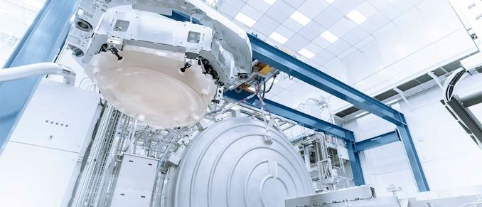
This week ASML is making two very important announcements related to their progress with high numerical aperature extreme ultraviolet lithography (High-NA EUV). First up, the company's High-NA EUV prototype system at its fab in Veldhoven, the Netherlands, has printed the first 10nm patterns, which is a major milestone for ASML and their next-gen tools. Second, the company has also revealed that it's second High-NA EUV system is now out the door as well, and has been shipped to an unnamed customer. "Our High-NA EUV system in Veldhoven printed the first-ever 10 nanometer dense lines," a statement by ASML reads. "Imaging was done after optics, sensors and stages completed coarse calibration. Next up: bringing the system to full performance. And achieving the same results in the...
ASML Delivers First 2nm-Generation Low-NA EUV Tool, the Twinscan NXE:3800E
Our avid readers tend to look at microelectronics made using leading edge process technologies, which in case of Intel means usage of High-NA extreme ultraviolet (EUV) lithography a couple...
2 by Anton Shilov on 3/13/2024
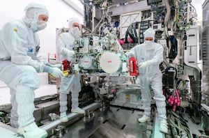
ASML's First High-NA EUV Litho Scanner Arrives At Intel [UPDATED]
Update 1/5/2024: Intel Oregon announced on Thursday that it has received its shipment of ASML's first-generation Twinscan EXE:5000 High-NA EUV lithography scanner. The two companies will start assembly process...
28 by Anton Shilov on 1/5/2024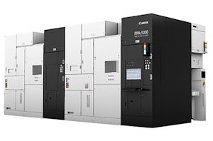
Canon Prepares Nanoimprint Lithography Tool To Challenge EUV Scanners
Canon has recently revealed its FPA-1200NZ2C, a nanoimprint semiconductor manufacturing tool that can be used to make advanced chips. The device uses nanoimprint lithography (NIL) technology as an alternative...
14 by Anton Shilov on 10/17/2023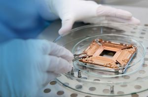
Intel Sells a 20% Stake in Maker of Multi E-Beam Mask Writing Tools
Intel on Wednesday announced that it had agreed to sell a 20% stake in IMS Nanofabrication, a company the develops and builds multi e-beam photomask writing tools, for $860...
1 by Anton Shilov on 6/22/2023
Intel Details PowerVia Chipmaking Tech: Backside Power Performing Well, On Schedule For 2024
At next week’s annual VLSI Symposium, Intel will be presenting a pair of highly-anticipated papers about their progress with their upcoming PowerVia chip fabrication technology – the company’s in-development...
31 by Ryan Smith on 6/5/2023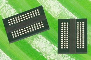
Micron to Bring EUV to Japan: 1γ Process DRAM to Be Made in Hiroshima in 2025
Micron this week officially said that it would equip its fab in Hiroshima, Japan, to produce DRAM chips on its 1γ (1-gamma) process technology, its first node to use...
10 by Anton Shilov on 5/19/2023
NVIDIA's cuLitho to Speed Up Computational Lithography for 2nm and Beyond
Production of chips using leading-edge process technologies requires more compute power than ever. To address requirements of 2nm nodes and beyond, NVIDIA is rolling out its cuLitho software library...
31 by Anton Shilov on 3/27/2023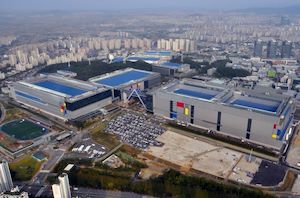
Samsung Seeks to Make South Korea No. 1 Chipmaker with $230B Investment Over 20 Years
Samsung on Wednesday unveiled their plan to invest $230 billion over the next 20 years in a new semiconductor production mega cluster in South Korea. The country's government believes...
22 by Anton Shilov on 3/15/2023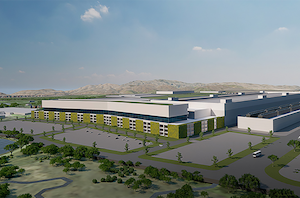
Micron Breaks Ground on Its $15 Billion EUV DRAM Fab in the U.S.
Micron this week broke ground on its leading-edge memory production facility near Boise, Idaho. The company will invest $15 billion in its new fab as a part of its...
23 by Anton Shilov on 9/14/2022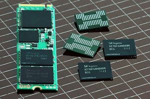
SK Hynix Starts Prepping for Next Semiconductor Boom with $11 Billion Memory Fab
When a major South Korean memory firm invests over $11 billion in a fab, that raises a couple of eyebrows. But when it comes within a major $100+ billion...
7 by Anton Shilov on 9/8/2022
Intel Kicks Off Fab Co-Investment Program with Brookfield: New Fabs to be Jointly Owned
Intel this week introduced its new Semiconductor Co-Investment Program (SCIP) under which it will build new manufacturing facilities in collaboration with investment partners – a sharp departure from the...
28 by Anton Shilov on 8/24/2022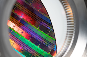
TSMC and ASML: Demand for Chips Remains Strong, But Getting Fab Tools Is Hard
TSMC's revenue this year is going to set an all-time record for the company, thanks to high demand for chips as well as increased prices that its customers are...
13 by Anton Shilov on 7/21/2022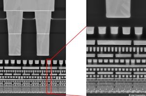
Intel 4 Process Node In Detail: 2x Density Scaling, 20% Improved Performance
Taking place this week is the IEEE’s annual VLSI Symposium, one of the industry’s major events for disclosing and discussing new chip manufacturing techniques. One of the most anticipated...
129 by Ryan Smith on 6/13/2022
Intel Discloses Multi-Generation Xeon Scalable Roadmap: New E-Core Only Xeons in 2024
It’s no secret that Intel’s enterprise processor platform has been stretched in recent generations. Compared to the competition, Intel is chasing its multi-die strategy while relying on a manufacturing...
147 by Dr. Ian Cutress on 2/17/2022
Texas To Get Multiple New Fabs as Samsung and TI to Spend $47 Billion on New Facilities
After a year of searching for the right place of its new U.S. fab, Samsung this week announced that it would build a fab near Taylor, Texas. The company...
135 by Anton Shilov on 11/24/2021
Bringing Geek Back: Q&A with Intel CEO Pat Gelsinger
One of the overriding key themes of Pat Gelsinger’s ten-month tenure at Intel has been the eponymous will to ‘bring geek back’ to the company, implying a return to...
49 by Dr. Ian Cutress on 10/29/2021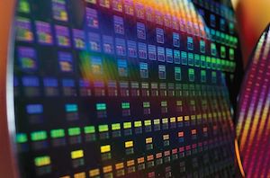
TSMC Roadmap Update: 3nm in Q1 2023, 3nm Enhanced in 2024, 2nm in 2025
TSMC has introduced a brand-new manufacturing technology roughly every two years over the past decade. Yet as the complexity of developing new fabrication processes is compounding, it is getting...
32 by Anton Shilov on 10/18/2021
Samsung Foundry: 2nm Silicon in 2025
One of the key semiconductor technologies beyond 3D FinFET transistors are Gate-All-Around transistors, which show promise to help extend the ability to drive processors and components to higher performance...
29 by Dr. Ian Cutress on 10/6/2021
Samsung Foundry to Almost Double Output by 2026
It’s hard not to notice that we’re in the middle of a semiconductor crunch right now. Factories are running at full steam, but pinch points in the supply chain...
6 by Dr. Ian Cutress on 10/6/2021


