Semiconductors
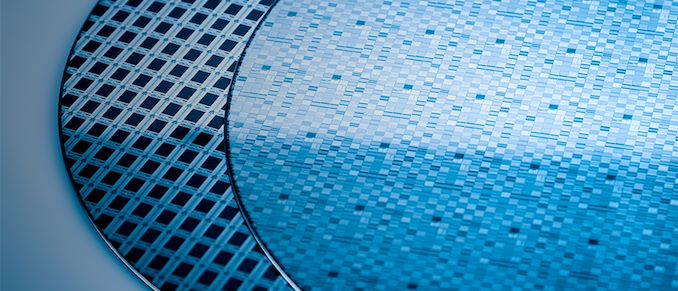
With the arrival of spring comes showers, flowers, and in the technology industry, TSMC's annual technology symposium series. With customers spread all around the world, the Taiwanese pure play foundry has adopted an interesting strategy for updating its customers on its fab plans, holding a series of symposiums from Silicon Valley to Shanghai. Kicking off the series every year – and giving us our first real look at TSMC's updated foundry plans for the coming years – is the Santa Clara stop, where yesterday the company has detailed several new technologies, ranging from more advanced lithography processes to massive, wafer-scale chip packing options. Today we're publishing several stories based on TSMC's different offerings, starting with TSMC's marquee announcement: their A16 process node. Meanwhile, for the...

Intel Calls Off Tower Acquisition, Forced to Focus Solely on Leading-Edge Nodes
Intel Corp. will not proceed with its $5.4 billion deal to acquire Tower Semiconductor foundry due to a lack of regulatory approval from China, the two companies announced on...
17 by Anton Shilov on 8/17/2023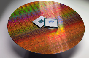
Intel and Synopsys Ink Deal to Develop IP for Intel's 3 and 18A Nodes
Intel and Synopsys this week signed an agreement under which Synopsys will develop a portfolio of various IP offerings for Intel 3 and 18A fabrication technologies for Intel Foundry...
1 by Anton Shilov on 8/15/2023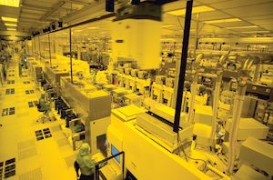
TSMC Establishes Joint Venture to Build 12nm/16nm Fab in Europe
TSMC on Tuesday announced plans to establish a European Semiconductor Manufacturing Company (ESMC) joint venture with its partners Bosch, Infineon, and NXP to build a fab near Dresden, Germany...
10 by Anton Shilov on 8/8/2023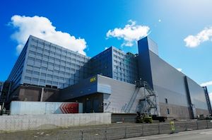
Intel Plans Massive Expansion in Oregon: D1X and D1A to Be Upgraded
Intel has filed a permit application that outlines significant expansion plans for its campus near Hillsboro, Oregon. According to filings submitted to state regulators, the tech giant's ambitious proposals...
4 by Anton Shilov on 8/2/2023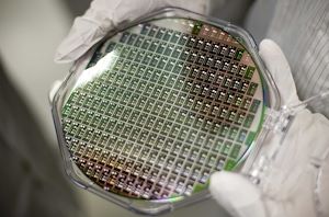
China Imposes New Export Restrictions on Gallium and Germanium
China this week formally imposed new export regulations on gallium and germanium, as well as materials incorporating them. This move is broadly seen as a retaliatory act for the...
6 by Anton Shilov on 8/2/2023
Dozens of Companies Adopt TSMC's 3nm Process Technology
Designing chips for modern, leading-edge manufacturing technologies is an expensive endeavor. Still, dozens of companies have already adopted TSMCs N3 and N3E (3 nm-class) fabrication processes, according to disclosures...
9 by Anton Shilov on 7/28/2023
Samsung Begins to Produce Third 3nm Chip Amid Massive Losses On DRAM & NAND
Samsung this week reported their financial results for the second quarter of 2023, closing the book on an especially bleak quarter of the year with a massive $3.4 billion...
14 by Anton Shilov on 7/28/2023
Rapidus Wants to Supply 2nm Chips to Tech Giants, Challenge TSMC
It has been a couple of decades since a Japanese fab has offered a leading-edge chip manufacturing process. Even to this day, none of the Japanese chipmakers have made...
19 by Anton Shilov on 7/26/2023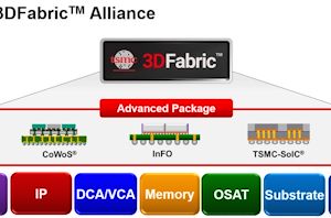
TSMC to Build $2.87 Billion Facility For Advanced Chip Packaging
TSMC on Tuesday announced plans to construct a new advanced chip packaging facility in Tongluo Science Park. The company intends to spend around $2.87 billion on the fab that...
3 by Anton Shilov on 7/25/2023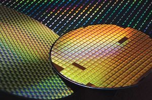
TSMC: 3nm Chips for Smartphones and HPCs Coming This Year
While TSMC formally started mass production of chips on its N3 (3nm-class) process technology late last year, the company is set to finally ship the first revenue wafers in...
21 by Anton Shilov on 7/21/2023
TSMC Delays Arizona Fab Deployment to 2025, Citing Shortage of Skilled Workers
TSMC on Thursday disclosed that it will have to delay mass production at its Fab 21 in Arizona to 2025, as a lack of suitably skilled workers is slowing...
27 by Anton Shilov on 7/20/2023
Samsung Shipping First GAAFET Silicon; 3nm and 4nm Yields Are Improving - Report
Currently, only two foundries offer their customers 3 nm and 4 nm-class process technologies: TSMC and Samsung Foundry. But business media sometimes blames Samsung Foundry for mediocre yields on...
5 by Anton Shilov on 7/18/2023
Intel Foundry Services Readies Intel 16 Process: Low Power FinFET For Everyday Chips
Intel Foundry Services (IFS) this week soft-launched their new Intel 16 process technology, a 16nm-class node that will be used for the production of low-power chips for everyday workloads...
3 by Anton Shilov on 7/14/2023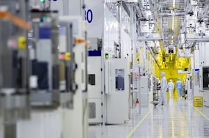
Samsung Updates Foundry Roadmap: 2nm in 2025, 1.4nm in 2027
Samsung Foundry revealed its latest process technology roadmap today at its annual Samsung Foundry Forum (SFF) 2023. The company's SF2 (2 nm-class) production node is on track for 2025...
4 by Anton Shilov on 6/27/2023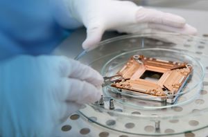
Intel Sells a 20% Stake in Maker of Multi E-Beam Mask Writing Tools
Intel on Wednesday announced that it had agreed to sell a 20% stake in IMS Nanofabrication, a company the develops and builds multi e-beam photomask writing tools, for $860...
1 by Anton Shilov on 6/22/2023
Intel to Spend Tens of Billions on New Fabs in Germany and Israel
Intel is spending tens of billions of dollars on new fabs in Arizona and Oregon, but the company's ambitions certainly do not end in the U.S. This month the...
28 by Anton Shilov on 6/21/2023
Top 10 Foundries See Revenue Drop Nearly 15% Year-over-Year
The top 10 contract makers of chips saw their Q1 2023 revenue decline by 14.6% year-over-year and 18.6% quarter-over-quarter, according to the most recent report by TrendForce. The market...
0 by Anton Shilov on 6/13/2023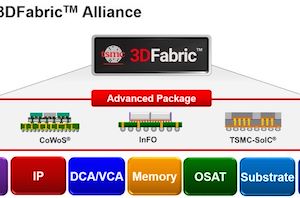
TSMC Opens Advanced Backend Packaging Fab for AI and HPC Products
TSMC on Friday formally opened its Advanced Backend Fab 6 facility, which it will be using to expand the company's capacity for building high-end, multi-chiplet products. The facility is...
1 by Anton Shilov on 6/9/2023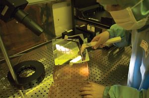
TSMC Shares More Info on 2nm: New MIM Capacitor and Backside PDN Detailed
TSMC has revealed some additional details about its upcoming N2 and N2P process technology at its European Technology Symposium 2023. Both production nodes are being developed with high-performance computing...
15 by Anton Shilov on 5/31/2023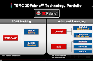
TSMC Preps 6x Reticle Size Super Carrier Interposer for Extreme SiP Processors
As part of their efforts to push the boundaries on the largest manufacturable chip sizes, Taiwan Semiconductor Manufacturing Co. is working on its new Chip-On-Wafer-On-Substrate-L (CoWoS-L) packaging technology that...
2 by Anton Shilov on 5/26/2023


