Google's Tensor inside of Pixel 6, Pixel 6 Pro: A Look into Performance & Efficiency
by Andrei Frumusanu on November 2, 2021 8:00 AM EST- Posted in
- Mobile
- Smartphones
- SoCs
- Pixel 6
- Pixel 6 Pro
- Google Tensor
Memory Subsystem & Latency
Usually, the first concern of a SoC design, is that it requires that it performs well in terms of its data fabric and properly giving its IP blocks access to the caches and DRAM of the system within good latency metrics, as latency, especially on the CPU side, is directly proportional to the end-result performance under many workloads.
The Google Tensor, is both similar, but different to the Exynos chips in this regard. Google does however fundamentally change how the internal fabric of the chip is set up in terms of various buses and interconnects, so we do expect some differences.
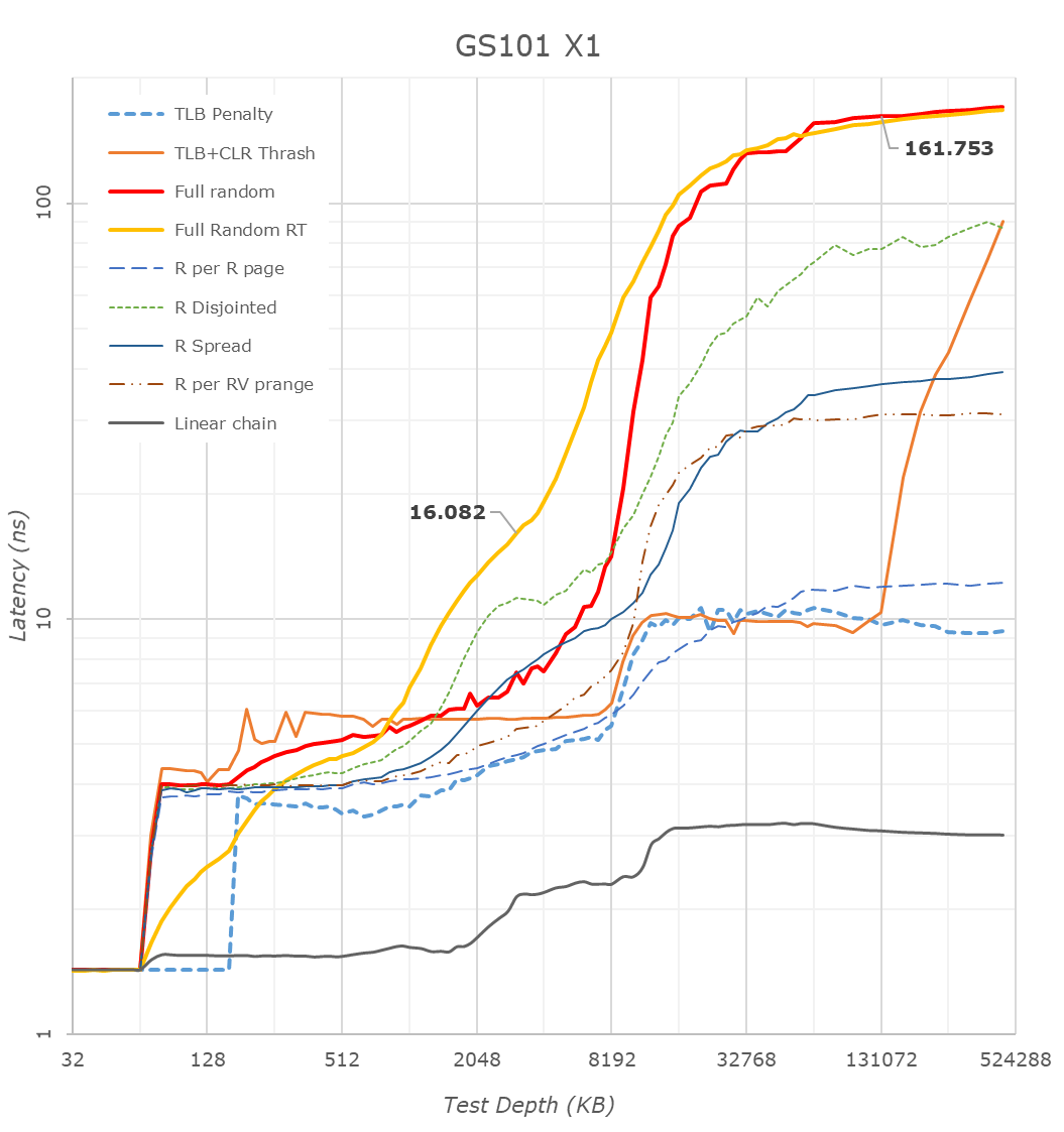
First off, we have to mention that many of the latency patterns here are still quite a broken due to the new Arm temporal prefetchers that were introduced with the Cortex-X1 and A78 series CPUs – please just pay attention to the orange “Full Random RT” curve which bypasses these.
There’s a couple of things to see here, let’s start at the CPU side, where we see the X1 cores of the Tensor chip being configured with 1MB of L2, which comes in contrast with the smaller 512KB of the Exynos 2100, but in line with what we see on the Snapdragon 888.
The second thing to note, is that it looks like the Tensor’s DRAM latency isn’t good, and showcases a considerable regression compared to the Exynos 2100, which in turn was quite worse off than the Snapdragon 888. While the measurements are correct in what they’re measuring, the problem is a bit more complex in the way that Google is operating the memory controllers on the Google Tensor. For the CPUs, Google is tying the MCs and DRAM speed based on performance counters of the CPUs and the actual workload IPC as well as memory stall % of the cores, which is different to the way Samsung runs things which are more transactional utilisation rate of the memory controllers. I’m not sure of the high memory latency figures of the CPUs are caused by this, or rather by simply having a higher latency fabric within the SoC as I wasn’t able to confirm the runtime operational frequencies of the memory during the tests on this unrooted device. However, it’s a topic which we’ll see brought up a few more times in the next few pages, especially on the CPU performance evaluation of things.
The Cortex-A76 view of things looks more normal in terms of latencies as things don’t get impacted by the temporal prefetchers, still, the latencies here are significantly higher than on competitor SoCs, on all patterns.
What I found weird, was that the L3 latencies of the Tensor SoC also look to be quite high, above that of the Exynos 2100 and Snapdragon 888 by quite a noticeable margin. I noted that one weird thing about the Tensor SoC, is that Google didn’t give the DSU and the L3 cache of the CPU cluster a dedicated clock plane, rather tying it to the frequency of the Cortex-A55 cores. The odd thing here is that, even if the X1 or A76 cores are under full load, the A55 cores as well as the L3 are still running at lower frequencies. The same scenario on the Exynos or Snapdragon chip would raise the frequency of the L3. This behaviour and aspect of the chip can be confirmed by running at dummy load on the Cortex-A55 cores in order to drive the L3 higher, which improves the figures on both the X1 and A76 cores.
The system level cache is visible in the latency hump starting at around 11-13MB (1MB L2 + 4MB L3 + 8MB SLC). I’m not showing it in the graphs here, but memory bandwidth on normal accesses on the Google chip is also slower than on the Exynos, but I think I do see more fabric bandwidth when doing things such as modifying individual cache lines – one of the reasons I think the SLC architecture is different than what’s on the Exynos 2100.
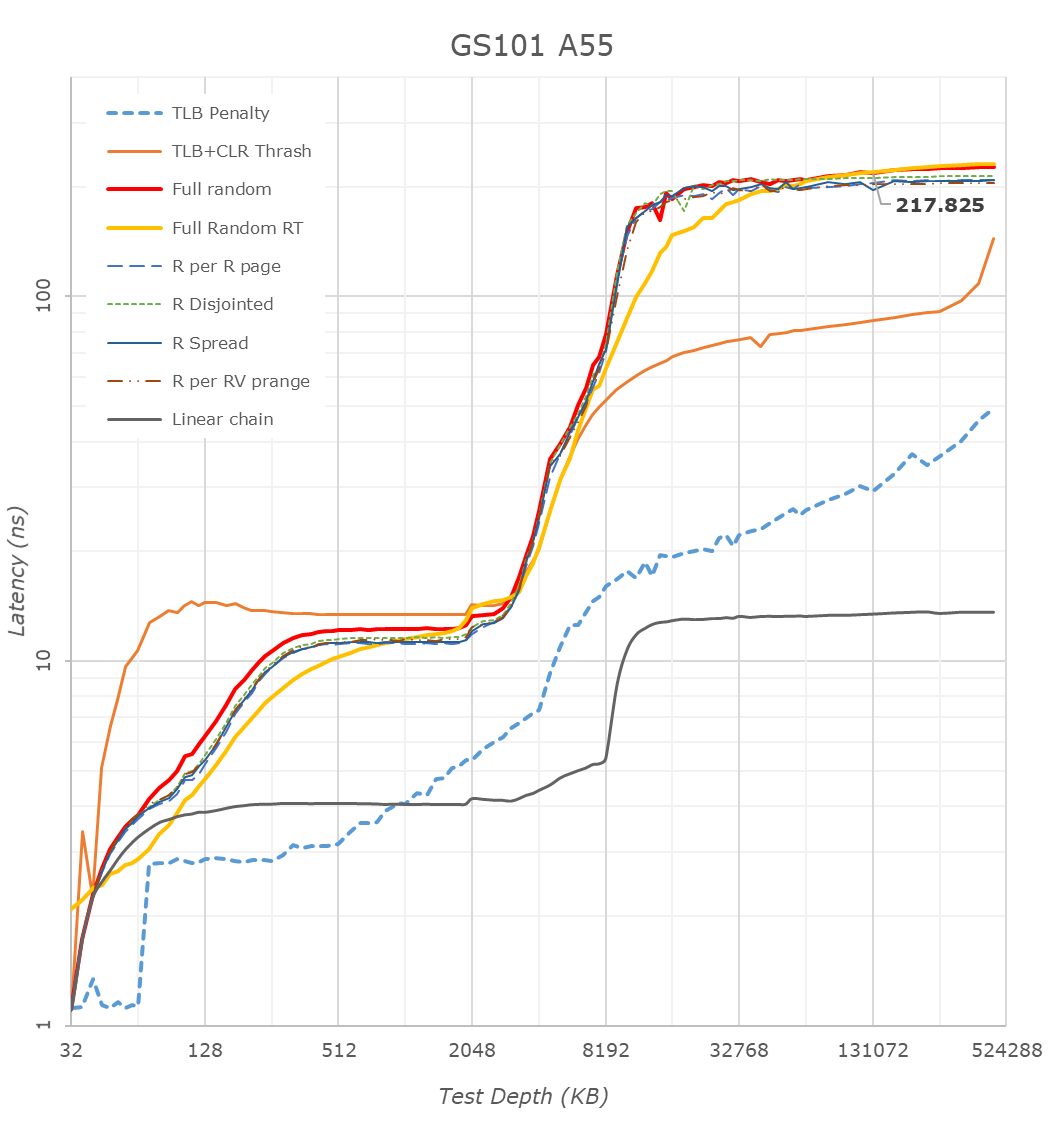
The A55 cores on the Google Tensor have 128KB of L2 cache. What’s interesting here is that because the L3 is on the same clock plane as the Cortex-A55 cores, and it runs at the same higher frequencies, is that the Tensor’s A55s have the lowest L3 latencies of the all the SoCs, as they do without an asynchronous clock bridge between the blocks. Like on the Exynos, there’s some sort of increase at 2MB, something we don’t see on the Snapdragon 888, and I think is related to how the L3 is implemented on the chips.
Overall, the Tensor SoC is quite different here in how it’s operated, and there’s some key behaviours that we’ll have to keep in mind for the performance evaluation part.


108 Comments
View All Comments
Speedfriend - Thursday, November 4, 2021 - link
The average laptop costs $500 and most expensive laptops are bought by enterprises where Mac OS has a limited share. While the Macbookz are great devices, they are hobbled by poor monitor support at the Air end and cray prices at the MacBook Pro end. For most users the difference between the performance of a MacBook Pro and a $1000 laptop is unnoticeable except in their wallet!dukhawk - Tuesday, November 2, 2021 - link
The chip is very Exynos design related. Looking through the kernel source and there are a ton of Exynos named files.dukhawk - Tuesday, November 2, 2021 - link
https://android.googlesource.com/device/google/rav...defaultluser - Tuesday, November 2, 2021 - link
If anyone wants to know know why Nvidia is most interested in purchasing ARM, it's in order to put the inefficient Mali out of it's misery - and simultaneously replace it with their own license-able Geforce cores!Since ARM Corp started throwing in the GPU for free, they've had to cut GPU research (to pay for the increasingly complex CPU cores, all of which come out of the same revenue box!) But Nvidia has the massive Server Revenue to handle this architecture-design mismatch; they will keep the top 50% of the engineers, and cut the other cruft loose!
melgross - Tuesday, November 2, 2021 - link
That may be a side effect. But the reason for purchasing g it would be maki g money, and controlling the market. Yes, it’s true that Nvidia wa t to control all graphics and to turn the GPU into the main programming aim.TheinsanegamerN - Tuesday, November 2, 2021 - link
If nvidia wanted to do that they could simply license ARM and make their own superior chip. The fact they have fallen flat on their face every time they have tried speaks volumes.they want ARM for patents and $$$, nothing more.
defaultluser - Wednesday, November 3, 2021 - link
When a place like Rockchip can sell an Arm chip bundled with Mali for Peanuts, you can understand why superior GPU wasn't enough to win Phone customers!You also need integrated modem if you ever want to compete with Qualcomm (not something Nvidia was willing to do).
But that bundling system has been shorting ARM Mali development for years (Qualcomm, Apple, and soon Samsung (via AMD) are all bringing better high-end options into the field - you know your performance/watt must be pathetic when a company like Samsung is getting desperate-enough to pay the cost of porting AMD GPU over to ARM architecture.
Kvaern1 - Sunday, November 7, 2021 - link
"If nvidia wanted to do that they could simply license ARM and make their own superior chip."''simply'
No, no one can simply do that anymore and only two companies can. NVidia just bought one of them.
melgross - Tuesday, November 2, 2021 - link
I’m wondering about several things here.I don’t see the reason for using the A76 cores being one of time. This is a very new chip. The competitors on the Android side have been out for a while. They use A78 cores. Samsung uses A78 cores. So time doesn’t seem to be the issuer here, after all it does use the X1. So I wonder if it isn’t the size of the core on this already large, crowded chip that’s a reason, and possibly cost. If the newer cores take up more area they would cost slightly more. These chips are going to be bought in a fairly small number. Estimates have it that last year, Google sold between 4 and 7 million phones, and that they’re doubling this year’s order. Either would still be small, and give no advantage to Google in volume pricing compared to other chip makers.
The second is that you have to wonder if Google is following the Apple road here. Apple, of course, designs many chips, all for their own use. Will Google keep their chips for their own use, assuming they’re as successful in selling phones as Google hopes, or will they, after another generation, or two, when the chip is more of their own IP, offer them to other Android phone makers, and if so, how will Samsung feel about that, assuming their contract allows it?
SonOfKratos - Tuesday, November 2, 2021 - link
I think they went for the A76 cores because of cost, like you said Tensor is already huge and the A78 or A77 cores would be more power efficient but they are also much bigger than the A76 on 5nm process. Even if they were to clock an A78 lower it would just be a waste of money and space on the chip for them. They probably had a specific budget for the chip which meant a specific die size. This is not Apple who is willing to throw as much money as they can to get the best performance per watt.The display was rumored to be an E5 display from Samsung display which is in their latest display so I don't know why Google is not pushing for higher brightness but it could be because of heat dissipation as well...I highly doubt Samsung gave Google their garbage displays lol Also Google does not utilize the variable refresh rate very well and it's terrible for battery life. I have also seen a lot of janky scrolling with 120Hz in apps like Twitter..it has hiccups scrolling through the timeline compared to my Pixel 3.
The modem is very interesting probably more so than Tensor, this is the first competition for Qualcomm in the US at least. A lot of people have been saying that the modem is integrated in Tensor but why would Google integrate a modem that does not belong to them in "their" chip? That's like asking Apple to integrate Qualcomm modems in their chip. Also Samsung pays Qualcomm royalties for 5G so they probably have a special agreement surrounding the sale and implementation of the modem. It is definitely not as power efficient as Qualcomm's implementation but it's Good start. I got 400+ Mbps on T-Mobile 5GUC outdoors and 200 Mbps indoors (I don't know which band). It surprisingly supports n258 band like the iPhone.