TSMC's 1.6nm Technology Announced for Late 2026: A16 with "Super Power Rail" Backside Power
by Anton Shilov on April 25, 2024 7:30 AM EST
With the arrival of spring comes showers, flowers, and in the technology industry, TSMC's annual technology symposium series. With customers spread all around the world, the Taiwanese pure play foundry has adopted an interesting strategy for updating its customers on its fab plans, holding a series of symposiums from Silicon Valley to Shanghai. Kicking off the series every year – and giving us our first real look at TSMC's updated foundry plans for the coming years – is the Santa Clara stop, where yesterday the company has detailed several new technologies, ranging from more advanced lithography processes to massive, wafer-scale chip packing options.
Today we're publishing several stories based on TSMC's different offerings, starting with TSMC's marquee announcement: their A16 process node. Meanwhile, for the rest of our symposium stories, please be sure to check out the related reading below, and check back for additional stories.
- TSMC's 1.6nm Technology Announced for Late 2026: A16 with "Super Power Rail" Backside Power
- TSMC 2nm Update: N2 In 2025, N2P Loses Backside Power, and NanoFlex Brings Optimal Cells
- TSMC Preps Cheaper 4nm N4C Process For 2025, Aiming For 8.5% Cost Reduction
- TSMC's System-on-Wafer Platform Goes 3D: CoW-SoW Stacks Up the Chips
- TSMC Jumps Into Silicon Photonics, Lays Out Roadmap For 12.8 Tbps COUPE On-Package Interconnect
- TSMC Readies 8x Reticle Super Carrier Interposer For Next-Gen Chips Twice as Large As Today's
Headlining its Silicon Valley stop, TSMC announced its first 'angstrom-class' process technology: A16. Following a production schedule shift that has seen backside power delivery network technology (BSPDN) removed from TSMC's N2P node, the new 1.6nm-class production node will now be the first process to introduce BSPDN to TSMC's chipmaking repertoire. With the addition of backside power capabilities and other improvements, TSMC expects A16 to offer significantly improved performance and energy efficiency compared to TSMC's N2P fabrication process. It will be available to TSMC's clients starting H2 2026.
TSMC A16: Combining GAAFET With Backside Power Delivery
At a high level, TSMC's A16 process technology will rely on gate-all-around (GAAFET) nanosheet transistors and will feature a backside power rail, which will both improve power delivery and moderately increase transistor density. Compared to TSMC's N2P fabrication process, A16 is expected to offer a performance improvement of 8% to 10% at the same voltage and complexity, or a 15% to 20% reduction in power consumption at the same frequency and transistor count. TSMC is not listing detailed density parameters this far out, but the company says that chip density will increase by 1.07x to 1.10x – keeping in mind that transistor density heavily depends on the type and libraries of transistors used.
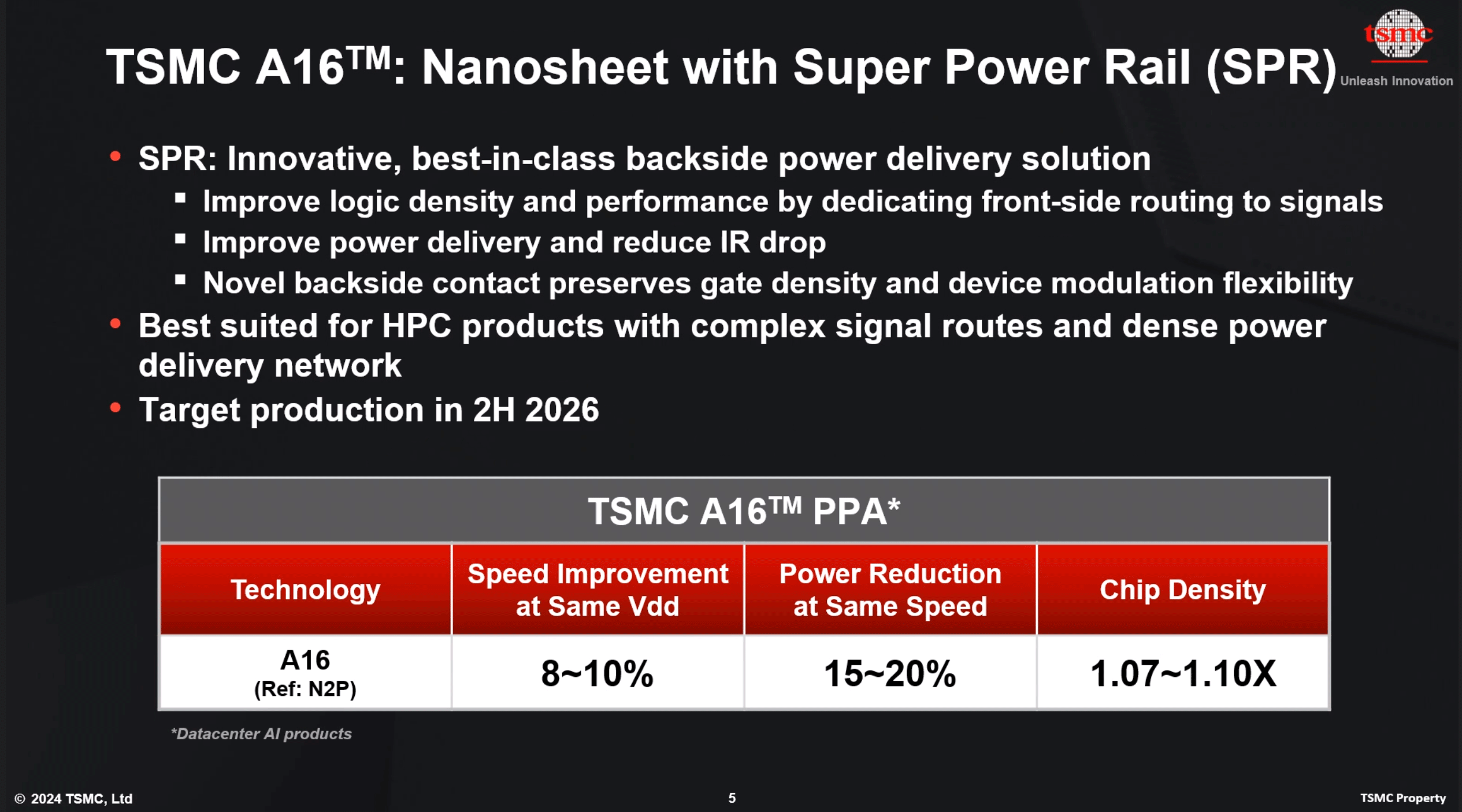
The key innovation of TSMC's A16 node, is its Super Power Rail (SPR) backside power delivery network, a first for TSMC. The contract chipmaker claims that A16's SPR is specifically tailored for high-performance computing products that feature both complex signal routes and dense power circuitry.
As noted earlier, with this week's announcement, A16 has now become the launch vehicle for backside power delivery at TSMC. The company was initially slated to offer BSPDN technology with N2P in 2026, but for reasons that aren't entirely clear, the tech has been punted from N2P and moved to A16. TSMC's official timing for N2P in 2023 was always a bit loose, so it's hard to say if this represents much of a practical delay for BSPDN at TSMC. But at the same time, it's important to underscore that A16 isn't just N2P renamed, but rather it will be a distinct technology from N2P.
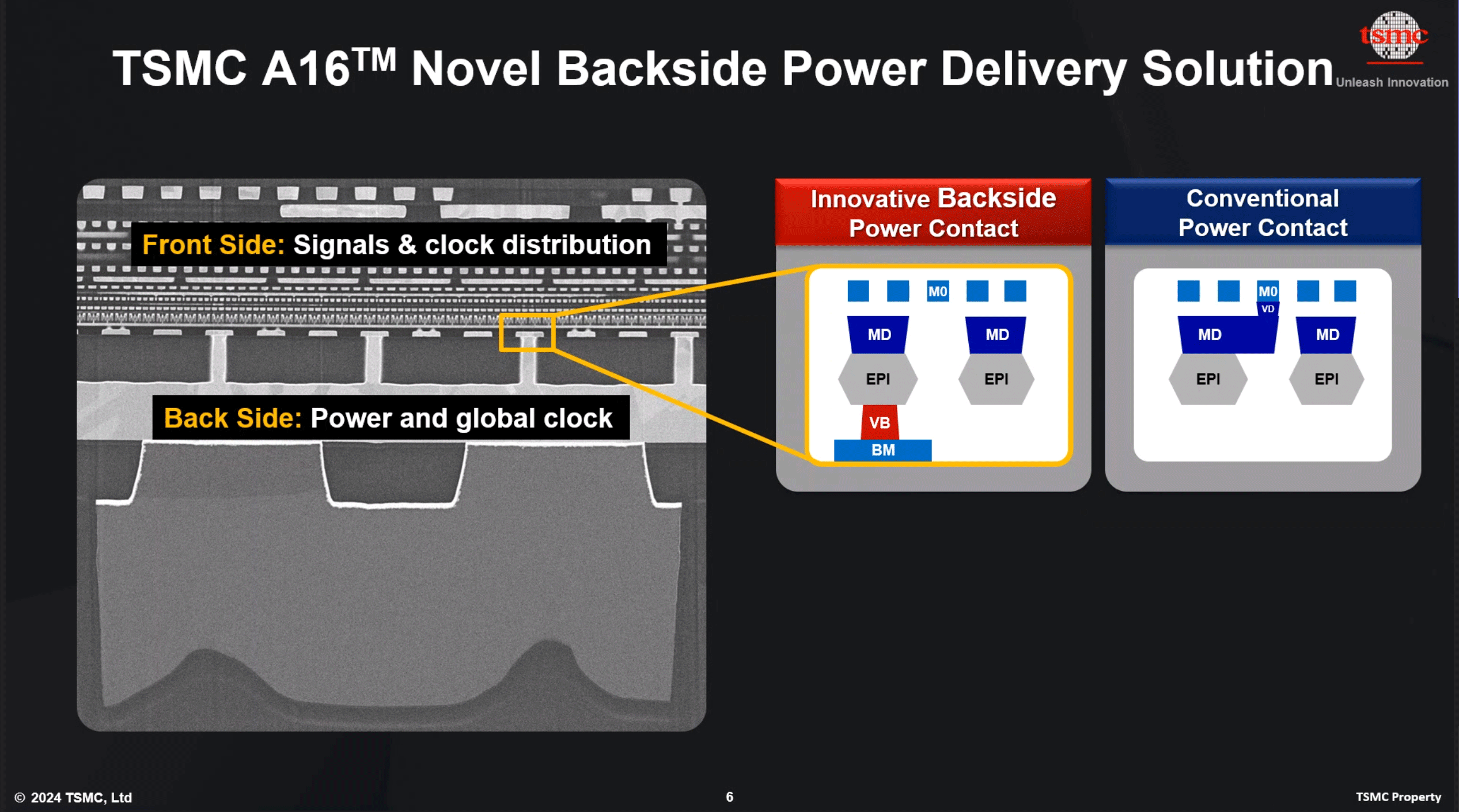
TSMC is not the only fab pursuing backside power delivery, and accordingly, we're seeing multiple variations on the technique crop up at different fabs. The overall industry has three approaches for BSPDN: Imec's Buried Power Rail, Intel's PowerVia, and now TSMC's Super Power Rail.
The oldest technique, Imec's Buried Power Rail, essentially places power delivery network on the backside of the wafer and then connects power rail of logic cells to power contact using nano TSVs. This enables some area scaling and does not add too much complexity to production. The second implementation, Intel's PowerVia, connects power to the cell or transistor contact, which provides a better result, but at the cost of complexity.
Finally, we have TSMC's new Super Power Rail BSPDN technology, which connects a backside power network directly to each transistor's source and drain. According to TSMC, this is the most efficient technology in terms of area scaling, but the trade-off is that it's the most complex (and expensive) when it comes to production.
That TSMC has opted to go with the most complex version of BSPDN may be part of the reason that we've seen it removed from N2P, as implementing it will ultimately add to both time and costs. This leaves A16 as TSMC's premiere performance node for the 2026/2027 time-frame, while N2P can be positioned to offer a more balanced combination of performance and cost efficiency.
Angstrom Era Kicks Off In Late 2026 With New Node Naming Convention
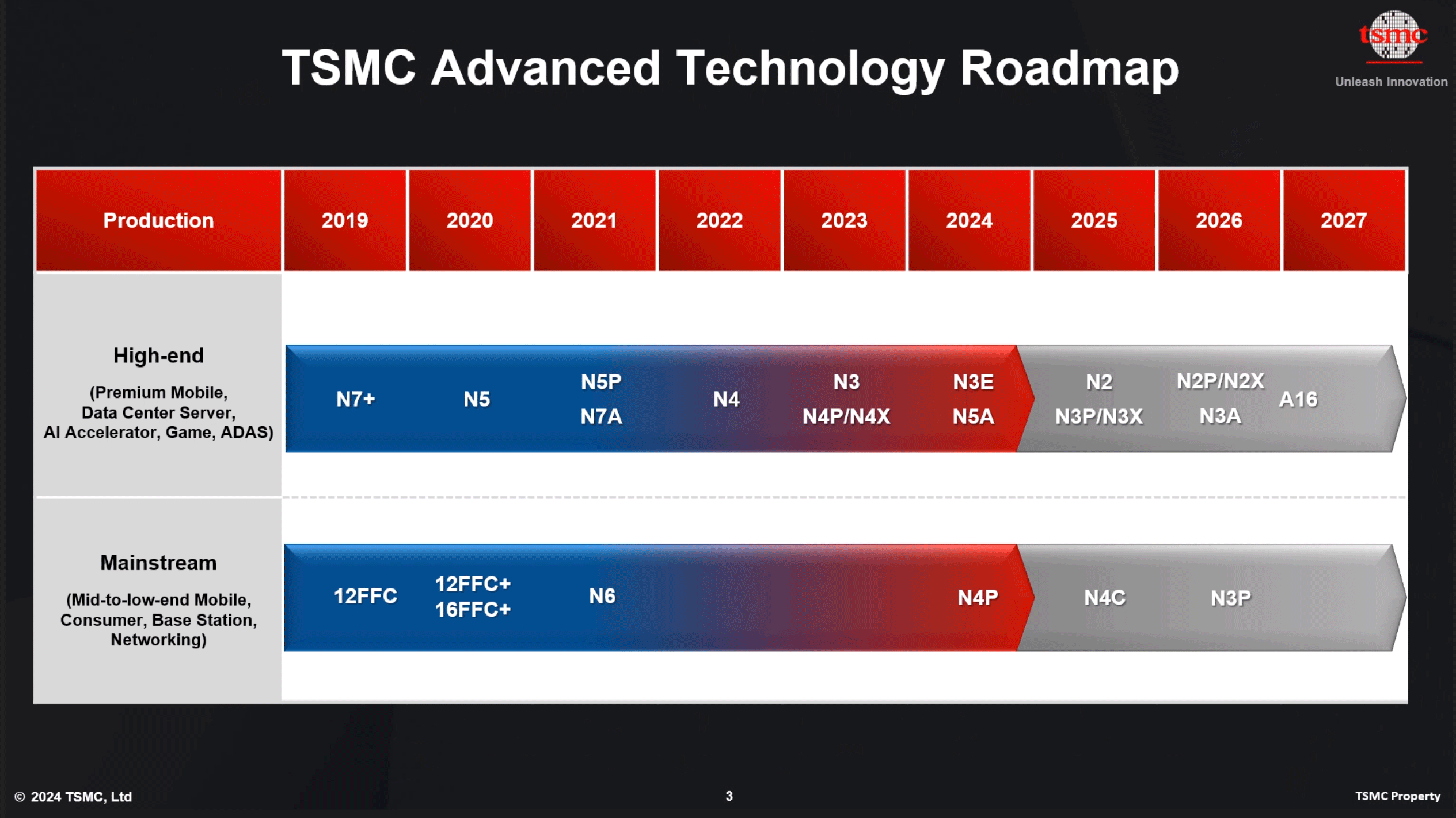
Finally, as with Intel, we're also seeing TSMC adopt a new process node naming convention starting with this generation of technology. The name itself is largely arbitrary – and this has already been the case in the fab industry for several years now – but with current node names already in the single digits (e.g. N2), the industry has needed to re-calibrate node names to something smaller than the nanometer. And thus we've arrived at the 'angstrom era.' But regardless of what exactly it's called or why it's called that, the important point is that A16 will be the next generation node beyond TSMC's 2nm-class products.
TSMC expects to start volume production on A16 in H2 2026, so it is likely that the first products based on this technology will hit the market in 2027. Given the timing, the production node will presumably compete against Intel's 14A; though at 2+ years out and with no one producing BSPDN in volume today, there's still a lot of time for plans and roadmaps to change.


18 Comments
View All Comments
ijdat - Saturday, April 27, 2024 - link
A16 *is* N2P-SPR renamed (to match Intel?), with the schedule brought in. The transistor and topside metal design rules are the same as N2P. The area and speed improvements are for HPC chips with dense power grids. ReplyRudde - Monday, April 29, 2024 - link
Yeah, it feels like a response to Intel renaming nodes. Essentially, A16 is a half-node to compete with Intel's 18A and 14A (half-)nodes. ReplyCiccioB - Tuesday, April 30, 2024 - link
<blockquote>The company was initially slated to offer BSPDN technology with N2P in 2026, but for reasons that aren't entirely clear, the tech has been punted from N2P and moved to A16.</blockquote>Well, it seems quite easy to understand what they did.
They planned a new PP they name N2 with Back Side Power which was going to be available in 2026 as for their roadmap.
They thought that being so ahead of Intel that was still stuck with their disastrous 10nm class PP would have given them enough advantage to slip a new PP with advanced features up to that date. They thought that a year late N3 was not a problem so a further year late N2 (with proper new techs) would also not be. So Back Side Power delivery has been adopted to be ready not earlier than 2026 (engineering generally needs its own time even if you put 10.000 men doing the job) and that is the date (at best, anything may always go not as planned).
Unfortunately for them, once Intel got rid of that catastrophic PP and started investing in the new advanced PP with a step by step method (like TSMC had done) they have shown an acceleration that could not be foresaw.
In less that 3 year Intel has almost closed the gap and is now launched to surpass TSMC with High NA-EUV, PowerVia and more advanced packaging (High NA-EUV is another thing TSMC is going to be left behind).
TSMC has foreseen that in 2025/2026 some customer may find Intel PPs much better for them, both under the point of technology but also availability, when Apple constantly usurps TSMC top node just for itself leaving almost nothing to others.
So what they did just not to be without anything new for almost 2 years?
They simply created an intermediary PP which is now called N2 and renamed the old N2 in A16 (how original!).
The new N2 is simply a small optical shrink (maybe achieved by adding more and more multi patterning layer) with no other particular innovations which is just there to attract customers that do not want to completely redesign a chip for the new technologies available by the competitor.
Will they succeed in that? Well, if Intel is able to offer a PP which is even similar to that offered by TSMC but with the production capabilities that TSMC cannot provide (due to Apple, as already said), I think many current customers will migrate to Intel PP to be able to advance to the latest nodes. One of them may be Nvidia, that had to release Blackwell with N4 instead of N3 because TSMC cannot offer it to anyone but Apple (and it seems it is not going that well in terms of yields with Apple now paying only the good chips). Qualcomm, Mediatek and others could follow. Reply
name99 - Tuesday, April 30, 2024 - link
No, N2 is NOT a "simply a small optical shrink" which shows your analysis is utterly worthless.The point of N2, the tech that it will prototype, is GAA.
TSMC is doing what they ALWAYS do, introducing a new technology in the context of an otherwise mostly unchanged stack, so as to minimize risk. Same way they introduced finFET as "N16", on top of what was mostly the N20 technology stack. Same reason they are not introducing BSPD in the same process that they introduce GAA. Reply
CiccioB - Tuesday, April 30, 2024 - link
They need to anticipate part of the innovations they wanted to offer together in the same original N2 which they wanted to offer in 2026 (as of old roadmap).But as said Intel is advancing too fast even for them, so they need to provide something meanwhile the BDPD becomes available.
Also, their original numbers with respect to N3 were very different (much worse) while now without BSPD they are giving better relative enhancements.
I suppose this move is just for trying to keep customers but in reality they will not achieve them initially.
It is all in the same information TSMC just gave themselves. Ignoring one part to accept the other is just cherry picking what we want to believe to.
Facts are that TSMC changed its plans to offer less technology earlier but incredibly with better enhancements than they announced with the PP with all new technologies together. This shows something is amiss, be it the sudden change of date for a different PP with the same name or for the data provided.
At the end it seems Intel is really scaring TSMC which is now late on many crucial new technologies. Reply
OreoCookie - Saturday, May 4, 2024 - link
Apart from the switch to GAAFETs, which name_99 has already mentioned, you wrote that Intel is ahead of TSMC when it comes to high-NA EUV. I think we need to consider cost here, adoption of high-NA EUV will lead to much higher cost and e. g. Semianalysis’ cost analysis states that high-NA EUV becomes economically viable much later than when it is slated for HV production at Intel. Maybe Intel is right and TSMC wrong, but it isn’t as clear cut. What use is a technologically superior but financially ruinous node to Intel? It also would most likely mean that designs need to fit in half a pre-high-NA reticle. Apple’s Max-series chips would be too large, for instance. A chip with the same (or larger) total area would need chiplets connected by EMIB or an interposer.Intel is making a bet, because they have to, while TSMC is playing it safer. Or perhaps Intel wants to attract customers like Apple that are willing and able to pay extra. I like the added competition. Intel is hungry and ambitious. Success is not guaranteed, but I think they are playing their cards well. But so is TSMC. Reply
my_wing - Wednesday, May 8, 2024 - link
As you guys said, do some more research.High NA EUV is suffered by the same thing when EUV started "Light source" i.e. the increase power to Light source to make the through put faster.
The point is that the High NA EUV machine Intel is having now is not a production lab, what is doing is that they "Intel and ASML" try to test all the system settings and as the Late Paul Otellini (Tick Tok@intel) copy exact to production sites.
I saw what you say i.e. the SemiAnalysis, that website to me sound too much like an TSMC PR. They can even say that TSMC N3P is better than Intel 18A. I am speechless, the most speechless is that Intel arrow lake should be in the Non Disclose Agreement Channel before the article written. Now that Rumor and "leaked" benchmark indicate that Arrow Lake Clock @ 5.5 GHz, sorry, where is TSMC lead, Size (remember BSPD lead to Gain of 6-10% so I don't see N3P can be denser than 18A).
Back to the point High-NA EUV, ASML (new) CEO already mentioned that their machine ever produce 80% still in production. The most critical point of economics here is throughput, ASML mentioned that they will continuous support and upgrade i.e. light source; in these world there are too many people going for hypes, even Bloomberg "Oh the US surrender the EUV opportunities La La La, but the US is still the supplier of the EUV light source to ASML.
I am a qualified accountant, when talk about EUV cost I am also an expert, the EUV machine at Intel should not be more than and Developmental machines, testing our processes, introducing 14A, 10A, etc etc. testing out new customer mask etc etc. even the throughput is slow, it just not that matter.
The report ignore the fact that the Light source will be continuously upgrade and the module will be replace (light source I think is similar to light bulb needed to replace after useful life), then the new upgraded module will be install and the through put is going to be higher.
Next bit is High EUV NA and the size of the mask, that Intel is carry on hoping ASML can address.
Overall because light source is modular, the author in SemiAnalysis do not take it into account and based on current throughput, that is a big mistake. Reply
ironargonaut - Friday, May 10, 2024 - link
What is the difference between "transistor contact" and "transistor's source and drain"? I am not familiar with the term "transistor contact". Reply