Google's Tensor inside of Pixel 6, Pixel 6 Pro: A Look into Performance & Efficiency
by Andrei Frumusanu on November 2, 2021 8:00 AM EST- Posted in
- Mobile
- Smartphones
- SoCs
- Pixel 6
- Pixel 6 Pro
- Google Tensor
Google's IP: Tensor TPU/NPU
At the heart of the Google Tensor, we find the TPU which actually gives the chip is marketing name. Developed by Google with input and feedback by the team’s research teams, taking advantage of years of extensive experience in the field of machine learning, Google puts a lot of value into the experiences that the new TPU allows for Pixel 6 phones. There’s a lot to talk about here, but let’s first try to break down some numbers, to try to see where the performance of the Tensor ends up relative to the competition.
We start off with MLCommon’s MLPerf – the benchmark suite works closely with all industry vendors in designing something that is representative of actual workloads that run on devices. We also run variants of the benchmark which are able to take advantage of various vendors SDKs and acceleration frameworks. Google had sent us a variant of the MLPerf app to test the Pixel 6 phones with – it’s to be noted that the workloads on the Tensor run via NNAPI, while other phones are optimised to run through the respective chip vendor’s libraries, such as Qualcomm’s SNPE, Samsung’s EDEN, or MediaTek’s Neuron – unfortunately only the Apple variant is lacking CoreML acceleration, thus we should expect lower scores on the A15.
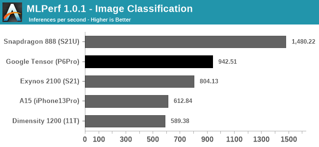
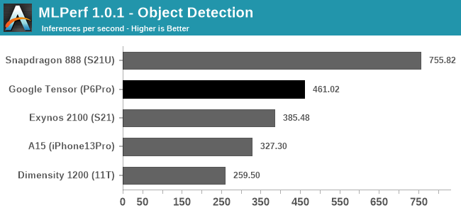
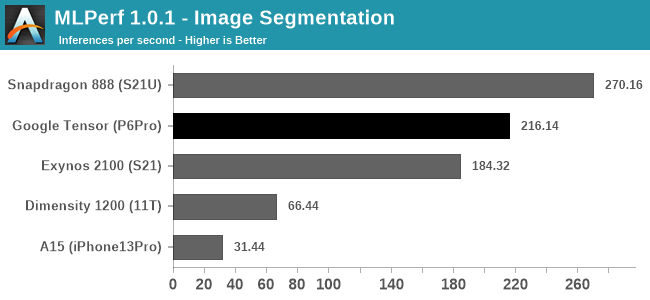
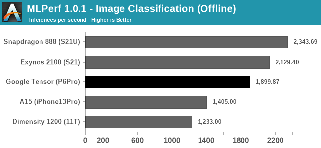
Starting off with the Image Classification, Object Detection, and Image Segmentation workloads, the Pixel 6 Pro and the Google Tensor showcase good performance, and the phone is able to outperform the Exynos 2100’s NPU and software stack. More recently, Qualcomm had optimised its software implementation for MLPerf 1.1, able to achieve higher scores than a few months ago, and this allows the Snapdragon 888 to achieve significantly better scores than what we’re seeing on the Google Tensor and the TPU – at least for those workloads, in the current software releases and optimisations.
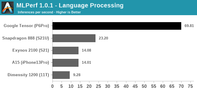
The Language Processing test of MLPerf is a MobileBERT model, and here for either architectural reasons of the TPU, or just a vastly superior software implementation, the Google Tensor is able to obliterate the competition in terms of inference speed.
In Google’s marketing, language processing, such as live transcribing, and live translations, are very major parts of the differentiating features that the new Google Tensor enables for the Pixel 6 series devices – in fact, when talking about the TPU performance, it’s exactly these workloads that the company highlights as being the killer use-cases and what the company calls state-of-the-art.
If the scores here are indeed a direct representation of Google’s design focus of the TPU, then that’s a massively impressive competitive advantage over other platforms, as it represents a giant leap in performance.
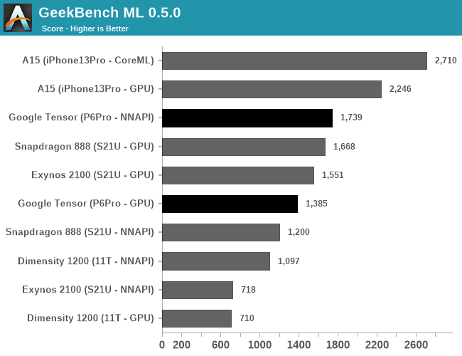
Other benchmarks we have available are for example GeekBench ML, which is currently still in a pre-release state in that the models and acceleration can still change in further updates.
The performance here depends on the APIs used, with the test either allowing TensorFlow delegates for the GPU or CPU, or using NNAPI on Android devices (and CoreML on iOS). The GPU results should only represent the GPU ML performance, which is surprisingly not that great on the Tensor, as it somehow lands below the Exynos 2100’s GPU.
In NNAPI mode, the Tensor is able to more clearly distinguish itself from the other SoCs, showcasing a 44% lead over the Snapdragon 888. It’s likely this represent the TPU performance lead, however it’s very hard to come to conclusions when it comes to such abstractions layer APIs.
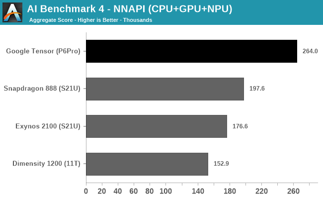
In AI Benchmark 4, when running the benchmark in pure NNAPI mode, the Google Tensor again showcases a very large performance advantage over the competition. Again, it’s hard to come to conclusions as to what’s driving the performance here as there’s use of CPU, GPU, and NPUs.
I briefly looked at the power profile of the Pixel 6 Pro when running the test, and it showcased similar power figures to the Exynos 2100, which extremely high burst power figures of up to 14W when doing individual inferences. Due to the much higher performance the Tensor showcases, it also means it’s that much more efficient. The Snapdragon 888 peaked around 12W in the same workloads, so the efficiency gap here isn’t as large, however it’s still in favour of Google’s chip.
All in all, Google’s ML performance of the Tensor has been its main marketing point, and Google doesn’t disappoint in that regard, as the chip and the TPU seemingly are able to showcase extremely large performance advantages over the competition. While power is still very high, completing an inference faster means that energy efficiency is also much better.
I asked Google what their plans are in regards to the software side of things for the TPU – whether they’ll be releasing a public SDK for developers to tap into the TPU, or whether things will remain more NNAPI centric like how they are today on the Pixels. The company wouldn’t commit yet to any plans as it’s still very early – in generally that’s the same tone we’ve heard from other companies as even Samsung, even 2 years after the release of their first-gen NPU, doesn’t publicly make available their Eden SDK. Google notes that there is massive performance potential for the TPU and that the Pixel 6 phones are able to use them in first-party software, which enables the many ML features for the camera, and many translation features on the phone.


108 Comments
View All Comments
jaju123 - Tuesday, November 2, 2021 - link
Thanks Andrei, using the P6 Pro right now and it is remarkably smooth in terms of general UI regardless of the benchmark scores etc., in comparison to other phones. I suspect the scheduling and UI rendering side of things are contributing here. Very much looking forward to the camera review!jiffylube1024 - Wednesday, November 3, 2021 - link
Same experience here on a P6 regular.I went from an S20 (regular) to the P6 pro. Wife has the S21 regular.
My experience so far:
UI is insanely fast and smooth on the P6. Everything is buttery smooth, no lag ever. It's a joy to use. The S20 is a very fast phone, but it did have the very occasional hiccup when switching between many different apps. So far, this hasn't happened on the Pixel 6 at all.
The S20 had nicer hardware overall, and the hand size was perfect. S20 screen gets a bit brighter, was a tiny bit sharper, and auto-adjust brightness was basically perfect on the S20, it's a little bit imperfect on the P6 (occasionally goes up or down in low light for no reason).
All in all, I'm very happy with the Pixel 6. If the Pixel 7 comes in a 6"-6.2" version next year, I may have to switch again, though!
Kangal - Wednesday, November 3, 2021 - link
That's because it is running a mostly Stock OS. Google severely limits background tasks when in use, and prioritises touch input... as opposed to say Samsung, which starts off slower and raises frequency in steps, whilst continuing background tasks. This slows the experience, but can boost efficiency, depending on the user.Now, the Cortex-A76 is actually not bad. It's a great chip, as it's quiet fast while being efficient. It requires less area and density compared to the A77 and A78. So Google didn't make a mistake here. By going for the A76, they were able to upgrade to have two Cortex-X1 cores. It is a design choice. Another design choice could be 3x X1 and 5x A55, cutting out the Middle-cores for a more simpler design. Or you could potentially have 4x A78 and 4x A55, and have the A78 cores clock higher, for better sustained performance than X1. These are all different design choices, one can be better than another, but it depends on the circumstances.
Kangal - Wednesday, November 3, 2021 - link
I just want to add my viewpoint on the performance and efficiency of this chipset/phone.AI/ML/NPU/TPU Benchmark: GeekBench ML 0.5
This looks like the most accurate representation. The iPhone 13 has an impressive AI performance because their SDK is better fleshed out, their software is coded more natively, and the SoC has pretty impressive specs Cache, CPU, GPU to help with such tasks. The GS101 wins in the Android ecosystem by a wide margin, followed by QSD 888, MediaTek Dimensity, then lastly Exynos. We can see the proper AI chart here: https://images.anandtech.com/graphs/graph17032/126...
GPU Benchmark: GFxBench Aztec Ruins High (Sustained)
This looks like the most accurate representation. Again Apple flexes its lead with its optimised software and cutting-edge hardware. Larger phones with better cooling manage to score higher, and giving preference to Qualcomm's mature drivers, followed by Huawei's node advantage, then the mediocre attempts by Exynos which is tied for the last spot with the GS101. We can see the proper GPU chart here: https://images.anandtech.com/graphs/graph17032/101...
CPU Multithread Benchmark: GeekBench 5 (crude Single/Multithread)
In the multi-thread test, it shows how sacrificing the middle cores has affected the total score, where it helps to boost the performance of the first 1-2 threads. So at least that design choice is captured. We can see the proper Multithread CPU chart here: https://images.anandtech.com/graphs/graph16983/116...
CPU Single-core Benchmark: SPEC 2017 (fp scores)
The SPEC test is more nuanced. We've established that Anandtech has made huge blunders here. Instead of reporting the Power Draw (watts) of the chipset, they instead try to calculate Energy Consumed (joules) by estimating it crudely. It is for that reason, we get some very inconsistent and wrong data. Such as Apple's Efficiency cores using less power than a Cortex-A53, yet producing scores in line with the Cortex-A78.
So instead, we will focus on the fp-scores instead of the int-scores, since this actually scales better from chipset to chipset. And we will focus on the Power Draw figures, to get the proper data. In particular, the tests of 526, 544, and 511 are quite revealing. We can see the proper CPU chart here:
https://images.anandtech.com/doci/16983/SPECfp-pow...
As a summary of the raw data, here:
Chipset-CoreType: Performance Value / Watts Recorded = Efficiency Score
Apple A14-E: 2.54 / 0.42 = 6.05
Apple A15-E: 3.03 / 0.52 = 5.83
Dim 1200-A55: 0.71 / 0.22 = 3.23
QSD 888-A55: 0.85 / 0.30 = 2.83
Exy 990-A55: 0.84 / 0.50 = 1.68 (? too low! Watts probably not recorded correctly)
Exy 2100-A55: 0.94 / 0.57 = 1.65 (? too low! Watts probably not recorded correctly)
GS 101-A55: 0.88 / 0.59 = 1.49 (? too low! Watts probably not recorded correctly)
Apple A15-P: 10.15 / 4.77 = 2.13
QSD 870-A77: 5.76 / 2.77 = 2.08
Apple A14-P: 8.95 / 4.72 = 1.90
QSD 888-X1: 6.28 / 3.48 = 1.80
GS 101-X1: 6.17 / 3.51 = 1.76
Dim 1200-A78: 4.71 / 2.94 = 1.60
Exy 2100-X1: 6.23 / 3.97 = 1.57
Exy 990-M5: 4.87 / 3.92 = 1.24
Andrei Frumusanu - Thursday, November 4, 2021 - link
> We've established that Anandtech has made huge blunders here. Instead of reporting the Power Draw (watts) of the chipset, they instead try to calculate Energy Consumed (joules) by estimating it crudely.I have no idea what you're referring to. The power draw is reported right there, and the energy isn't estimated, it's measured precisely. The A55 data is correct.
Perf/W is directly inversely relative to energy consumption if you would actually plot your data.
Kangal - Saturday, November 6, 2021 - link
The Specific Power Draw makes sense in the context of these comparisons. For the longest time in this industry, they've always talked about Performance per Watt. No-one, not even Intel (and they've been know to be quite shady) uses Performance per Joules.The total energy consumed in Joules is simply irrational. One can then make a flawed comparison of how much processing could be made through the consumption of a cupcake if you read it's nutritional content. Not only that, if you actually look at the data you guys submitted, it has a lot more variance with Joules, whilst Watts shows a lot more consistent results. Your energy consumed is an estimate, not what is specifically used by the cores when running.
For instance, when using Joules, it makes Apple's Efficiency cores seem to use slightly less power than a Cortex-A55, whilst performing benchmarks slightly faster than a Cortex-A76. If that is true, then no Android phones would be sold above $500 as everyone would simply buy iPhones. It's like comparing a 2011 processor (48nm Dual Cortex-A9) to a 2015 processor (16nm Octa Cortex-A53), so it's not only using less power, but delivering more than x4 times the performance. Ludicrous. You just cannot magically wave away discrepancies that big (x7.43). On the other hand, if you plot it using Watts, you get a deeper picture. Apple's Efficiency cores use about double the energy as a Cortex-A55 but in turn they deliver four times the performance, so the net difference is a much more palatable x2.14 leap in efficiency (at least in max performance comparison). And I'm comparing the latest Apple (A15) to Android (QSD 888) cores.
If the A55 data is as accurate as you say, why do you have discrepancies there as well?
For example, QSD 888 versus Google Silicon-101... they're both using off-the-shelf Cortex-A55. Yet, the Qualcomm's chipset is apparently drawing only 0.30 Watts, compared to 0.59 Watts... which is about x2 less. And both perform fairly close scores at 0.85 versus 0.88, making their total efficiency difference of x1.90 (2.83 vs 1.49) puzzling. So something is a miss. Going off the Joules Estimates doesn't fix the issue either, as you still have an unaccounted x1.83 difference in efficiency still.
With all your resources, you guys never got curious about such discrepancies?
(sorry for being a little obtuse)
dotjaz - Sunday, November 7, 2021 - link
You are obviously uneducated, and don't know what "off-the-shelf" means in any chips. Physical implementation varies a lot even on the same process with the same IP. Either you or Cadence are lying. I'd rather believe a reputable company with decades of experience.https://www.anandtech.com/show/16836/cadence-cereb...
Kangal - Sunday, November 7, 2021 - link
Snapdragon 888: 4x Cortex-A55 @ 1.80GHz 4x128KB pL2, with 4MB sL3, on Samsung5nm (5LPE)
Google Tensor: 4x Cortex-A55 @ 1.80GHz 4x128KB pL2, with 4MB sL3, on Samsung
5nm (5LPE)
Both of these SoC's are using Cortex-A55 cores which were licensed from ARM directly. They are off-the-shelf. These are not custom cores, such as the Mongoose, Early-Kyro, Krait, Denver, Carmel, or the 8-or-so different custom designs released by Apple. If you say that I am lying, then you are also saying that both Google, Qualcomm, are also lying. And note, that they are virtually identical in their specifications and build.
I think you entirely mis-understood the point of Cadence is about. Sure, even on the same chips there are variance, the so-called "silicon lottery". But be realistic, how much of a difference do you think it is? I'll give a hint, the larger the silicon, the more the variance, and the bigger the difference. If you check the latest data from the now bankrupt siliconlottery.com service, the difference with the 3950X is (worst) 4.00Ghz versus 4.15Ghz (best). At best that is a 3-point-something-percent difference, so let's say it is 5%... and this difference is likely to be less on smaller chips. But even if we accept 5%, that is nowhere near x2 variance.
Also, you would be calling AnandTech liars as well:
" the new Cortex-A77 picks up where the Cortex-A76 left off and follows Arm’s projected trajectory of delivering a continued SOLID PERFORMANCE UPLIFT of 20-25% CAGR "...
How is it that we are able to be impressed by a +20% uplift, yet, we completely disregard a +90% difference? It is not logical, and doesn't pass the sniff test. You can call me uneducated all you like, I'm trying to arrive at the truth, since there are big discrepancies with the data provided that I've pointed out to above. I am open to criticism, as everyone should be.
TellowKrinkle - Tuesday, November 9, 2021 - link
Let's look at some unitsPerformance is units of calculation work divided by time. For our graph, some constant times spec runs per second.
Performance per watt is then some constant times (spec runs) / (seconds * watts)
The joules measurement put up there is specifically joules per spec run. One joule is one watt second, so that number would therefore be (watts * seconds) / (spec runs).
Notice the similarity? Joules is 1/(perf per watt).
Hopefully it's clear from this that the "joules" measurement on that graph *is* there to indicate efficiency, just like a perf/watt measurement would be. The only difference is that in the joules graph, high numbers indicate inefficient processors, while in a perf/watt graph, those would be represented by low numbers.
The0ne - Thursday, November 4, 2021 - link
Pixel 4A updated last night to 12 and it runs even smoother. The UI tricks they have done does appear to make a visual difference. So far I'm impressed with 12 aside from the gigantic texts and bars here and there.