TSMC Boosts CapEx by $1 Billion, Expects N5 Node to Be Major Success
by Anton Shilov on January 22, 2020 11:15 AM EST
TSMC is on track to begin high-volume production of chips using its 5 nm technology in the coming months, the company said in its conference call last week. While so far the number of 5 nm tape-outs is lower when compared to the number of 7 nm tape-outs several months before production start, TSMC expects the process to become a major commercial success. Meanwhile, to ensure that it has no production constraints, the company plans to increase its 2020 CapEx by $1 billion.
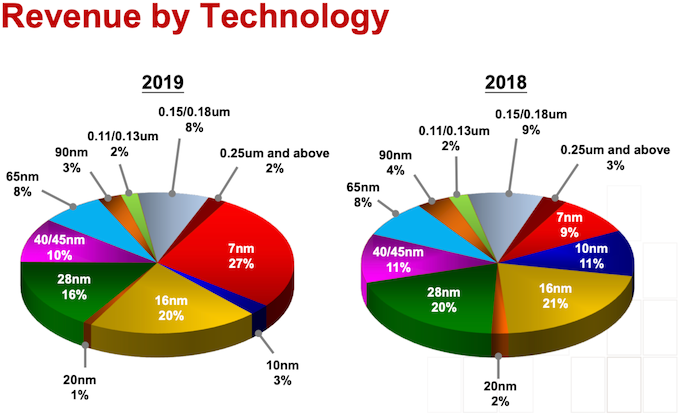
It is well known that TSMC’s N5 manufacturing technology provides substantial improvements over the company’s N7 fabrication process (1.8x higher transistor density, +15% frequency or -20% power consumption), so major customers of the company are more than inclined to adopt it. TSMC is on track to start high volume manufacturing (HVM) using the technology in the first half of this year. So far, the number of N5 tape-outs is lower when compared to the number of N7 tape-outs at the same stage of development (i.e., several months before HVM) becase alpha customers have taped out a slightly lower number of N5 designs and other clients are yet to catch up. Meanwhile, TSMC remains optimistic about the technology’s ramp and expects N5 revenue to account for 10% of its 2020 wafer sales revenue, which essentially means that business performance of N5 in its first year will be the same as business performance of N7 in its first year.
There are several reasons why TSMC’s N7 node turned out to be a huge commercial success for the foundry. First up, most of its customers skipped the 10 nm node and were more than motivated to go with 7 nm. Secondly, TSMC did not have a strong competition with its N7 technology: GlobalFoundries pulled out of the 7 nm race, whereas Samsung Foundry hardly processed any significant number of wafers using its 7LPP process. Thirdly, because N7 is a considerably more complex technology than TSMC’s 16 nm or 10 nm nodes, the company charges more money per wafer than before, which drives a greater revenue share for the process.
C. C. Wei, Vice Chairman and CEO of TSMC said the following:
“The 5 nm tape-out is little bit less than 7 nm compared at the same stage of the time. However, the most important thing is that the high-volume tape-out is almost equal. So, we expect that our 5 nm ramp is a very fast and smooth and it will contribute about 10% to this year's revenue."
Since TSMC’s N7 is considered as a long-living node, demand for the process is not expected to drop radically when N5 enters HVM, as there are tens of fabless semiconductor developers waiting to produce their 7 nm designs. Apparently, to satisfy demand for chips made using TSMC’s N7, N7+, N7P, N6, N5, and N5P manufacturing technologies (and offer some additional capacity for specialty processes as well as for advanced packaging), the company will have to further increase its 2020 CapEx by a billion of dollars up from $14 billion - $15 billion estimated last year.
TSMC does not say exactly how the additional $1 billion will be spent, but since in the coming quarters it will be ramping production using four process technologies that that use extreme ultraviolet lithography (EUVL) for select layers (up to 14 layers in case of N5, up from 4 and 5 in case of N7+ and N6) and multipatterning for some others, it is likely that the foundry is going to need some additional leading-edge equipment.
Wendell Huang, VP and CFO of TSMC, said the following:
“Other than the advanced technology, we also mentioned earlier, we also increased the CapEx this year for specialty technology as well as advanced packaging. So those are the areas that we are focusing on.”
Related Reading:
- TSMC: 5nm on Track for Q2 2020 HVM, Will Ramp Faster Than 7nm
- TSMC Radically Boosts CapEx to Expand Production Capacities, To Reach $14B For 2019
- Early TSMC 5nm Test Chip Yields 80%, HVM Coming in H1 2020
- TSMC: N7+ EUV Process Technology in High Volume, 6nm (N6) Coming Soon
Source: TSMC


40 Comments
View All Comments
RSAUser - Sunday, January 26, 2020 - link
GPU is a lot more tolerant of faults, easier to fuse off and generally runs at a lower clock.Amandtec - Thursday, January 23, 2020 - link
Intel have other paths to win back CPU than node shrinks. If they can pull of a 3d stacked win it will work as well. If they do none of it, they are heading for mass layoffs and a stock price dive.FreckledTrout - Thursday, January 23, 2020 - link
I wouldn't bet against Intel. History has shown when Intel messes up they come back strong.Korguz - Thursday, January 23, 2020 - link
intel has been messing up for like 5 years now, when will they come back ??? they have also been lieing for about that long too...yeeeeman - Friday, January 24, 2020 - link
You say that because you don't understand a thing about manufacturing.Korguz - Friday, January 24, 2020 - link
maybe i dont. but a company like intel.. with all its money and personel.. cant get something to work ?? come on... 10nm must of been screwed up big time...Spunjji - Monday, January 27, 2020 - link
I'm inclined to disagree - I think they'll perform exactly the same sort of 7nm "release" in 2021 that they did with Cannon Lake, with a slow ramp into 2022.We'll see, though. At this stage in semiconductor development, I think it's safe to say that all bets are off.
ksec - Thursday, January 23, 2020 - link
1. Just like 10nm in 2019 from Intel, in reality it isn't any where near the volume you would expect. They barely ship it out in last quarter.2. When TSMC state 7nm, and HVM that means there will be 50M+ not only fabbed or shipped, but SOLD on the market. That is going like clock work from Apple.
So looking at years shipped doesn't realistically show the gap between Intel and TSMC.
I would point out again, ASML is the only EUV machines supplier. TSMC has been getting as many as they could, you could bet Intel 7nm won't have any volume from the start either.
Amandtec - Thursday, January 23, 2020 - link
Rumor has it they fell behind because they thought they could still progress to 10nm and beyond without buying expensive eternal tools (e.g. EUV tools).FreckledTrout - Thursday, January 23, 2020 - link
Well for 10nm it's not a rumor. They went with quad patterning which worked except scaling the frequencies was severely hampered. I have a feeling they were thinking EUV for 7nm all along as they were already working on it a long time ago.