TSMC Details 3nm Evolution: N3E On Schedule, N3P and N3X To Deliver 5% Performance Gains
by Anton Shilov on April 26, 2023 5:15 PM EST
Alongside some new announcements for their 2nm process node plans, TSMC has also released a progress and roadmap update for their N3 family process technologies at today's 2023 North American Technology Symposium. TSMC's final generation of FinFET-based process nodes, the N3 family is expected to remain around in some shape or form for many years to come as the densest node available for customers who don't need a more cutting-edge GAAFET-based process.
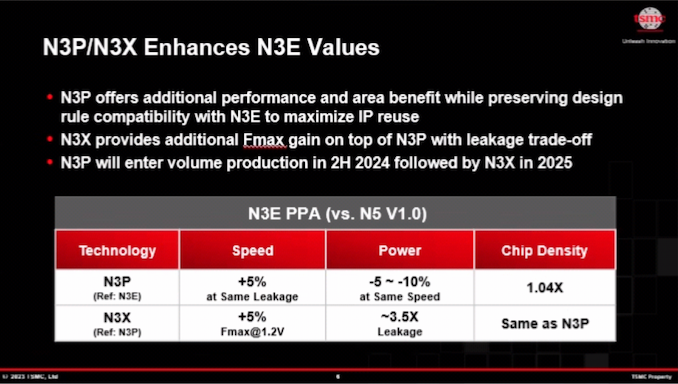
TSMC's big roadmap updates on the N3 front were with N3P and its high performance variant, N3X. As revealed today by TSMC, N3P will be an optical shrink of N3E, offering enhanced performance, reduced power consumption, and increased transistor density compared to N3E, all while maintaining compatibility with N3E's design rules. Meanwhile, N3X will wed extreme performance with 3nm-class densities, offering higher clockspeeds for high performance CPUs and other processors.
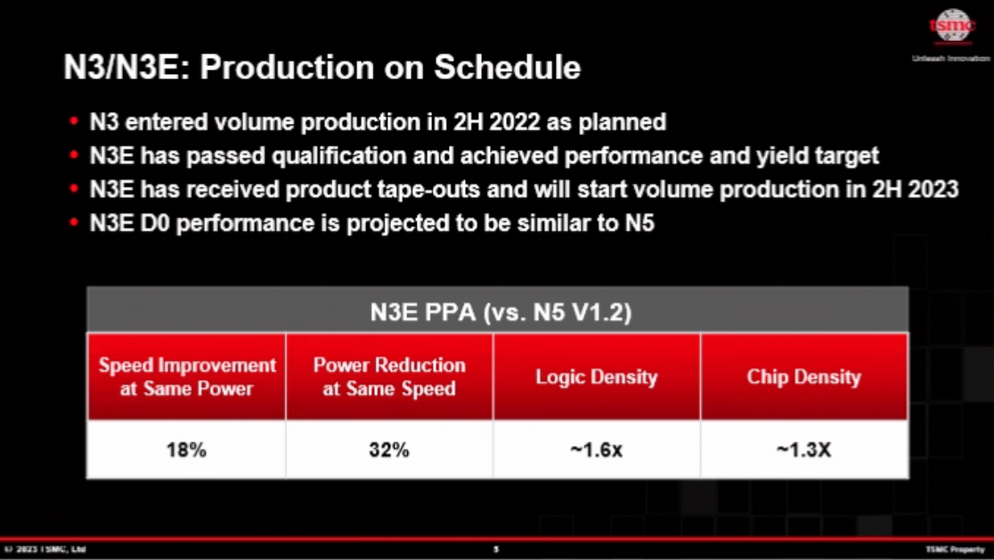
N3E: 3nm for Everyone Is on Schedule
As a quick refresher, TSMC's N3 (3nm-class) family of process technologies is comprised of several variants, including baseline N3 (aka N3B), relaxed N3E with reduced costs, N3P with enhanced performance and chip density, and N3X with higher voltage tolerances. Last year the company also talked about N3S with maximized transistor density, but this year the company remains tight lipped about this node and it is not mentioned anywhere in its slides.
TSMC's vanilla N3 node features up to 25 EUV layers (according to China Renaissance and SemiAnalysis), with TSMC using EUV double-patterning on some of them to make for higher logic and SRAM transistor density than N5. EUV steps are expensive in general, and EUV double patterning drives those costs up further, which is why this fabrication process is only expected to be used by a handful of customers who are not as concerned about the high outlay required.
| Advertised PPA Improvements of New Process Technologies Data announced during conference calls, events, press briefings and press releases |
|||
| TSMC | |||
| N3 vs N5 |
N3E vs N5 |
||
| Power | -25-30% | -32% | |
| Performance | +10-15% | +18% | |
| Logic Area Reduction* % Logic Density* |
0.58x -42% 1.7x |
0.625x -37.5% 1.6x |
|
| SRAM Cell Size | 0.0199µm² (-5% vs N5) | 0.021µm² (same as N5) | |
| Volume Manufacturing |
Late 2022 | H2 2023 | |
The majority of TSMC's clients interested in a 3nm-class process are expected to use the relaxed N3E node, which according to TSMC is on schedule and achieving their performance targets. N3E uses up to 19 EUV layers and does not rely on EUV double patterning at all (according to data from China Renaissance and SemiAnalysis), reducing its complexity and costs. The trade-off is that N3E offers lower logic density than N3, and it has the same SRAM cell size as TSMC's N5 node, making it somewhat less attractive to those customers who are driving for density/area gains. Overall, N3E promises a wider process window and better yields, which are two crucial metrics in chip fabrication.
"N3E will be better than N3 in terms of yield, process complexity, which directly translating into [wider] process window," said Kevin Zhang, Vice President of Business Development at TSMC.
N3P: Higher Performance, Higher Transistor Density
Following N3E, TSMC will continue to optimize the N3 family's transistor density with N3P, which will build on N3E by offering improved transistor characteristics. The refined process node will allow chip designers to either increase performance by 5% at the same leakage or reduce power by 5% ~ 10% at the same clocks. The new node will also increase transistor density by 4% for a 'mixed' chip design, which TSMC defines as a chip consisting of 50% logic, 30% SRAM, and 20% analog circuits.
As part of their discussion on N3P, TSMC stressed that the density improvement was achieved by adjusting the optical performance of its scanners. So it is likely that TSMC will be able to shrink all types of chip structures here, which will make N3P an attractive node for SRAM-intensive designs.
"N3P is a performance boost, it has a 5% higher performance, at least a 5% higher than N3E," explained Zhang. It also has the 2% optical shrink, which bring transistor density to 1.04x."
| Advertised PPA Improvements of New Process Technologies Data announced during conference calls, events, press briefings and press releases |
|||||
| TSMC | |||||
| N3 vs N5 |
N3E vs N5 |
N3P vs N3E |
N3X vs N3P |
||
| Power | -25-30% | -32% | -5% ~ 10% | higher | |
| Performance | +10-15% | +18% | +5% | +5% Fmax @ 1.2V |
|
| Chip Density | ? | ? | 1.04x | same | |
| SRAM Cell Size | 0.0199µm² (-5% vs N5) | 0.021µm² (same as N5) | ? | ? | |
| Volume Manufacturing |
Late 2022 | H2 2023 | H2 2024 | 2025 | |
Since N3P is an optical shrink of N3E, it will preserve N3E's design rules, enabling chip designers to quickly reuse N3E IP on the new node. Consequently, N3P is also projected to be one of TSMC's most popular N3 nodes, so expect IP design houses like Cadence and Synopsys to offer a variety of IP for this process technology, reaping the benefits of forward compatibility with existing N3E in the process. TSMC says that N3P will be production ready in the second half of 2024.
N3X: Maximum Performance and Density
Finally, for developers of high-performance computing applications like CPUs and GPUs, TSMC has for the past few generations been offering its X family of high voltage, performance-focused nodes. As disclosed at last year's event, the N3 family will be getting its own X variant with the aptly named N3X node.
Compared to N3E, N3X is projected to offer at least 5% higher clockspeeds compared to N3P. This is being accomplished by making the node more tolerant of higher voltages, allowing chip designers to crank up the clockspeeds in exchange for higher overall leakage.
TSMC claims that N3X will support voltages of (at least) 1.2v, which is a fairly extreme voltage for a 3nm-class fabrication process. The leakage cost, in turn, is significant, with TSMC projecting a whopping 250% increase in power leakage over the more balanced N3P node. This underscores why N3X is really only usable for HPC-class processors, and that chip designers will need to take extra care to keep their most powerful (and power-hungry) chips in check.
As for transistor density, N3X will offer the same density as N3P. TSMC has not commented on whether it will also maintain design rule compatibility with N3P and N3E, so it will be interesting to see what ends up happening there.
The final N3 family node in TSMC's current roadmap, the company says that that N3X will be production ready in 2025.
Source: TSMC


13 Comments
View All Comments
Wereweeb - Friday, April 28, 2023 - link
If Samsung didn't manage to make 3GAP outperform N3E they'd be in for some REAL trouble... Because it's comparing a GAAFET process to a FinFET process.It will be a little bit better but it'll be *much* more expensive to manufacture (More process steps + Sammy yields). TSMC knows that, they wanted that to happen - they know that by sticking to an optimised FinFET design they'll very soon start pushing out much higher volumes of wafers that beats Sammy's GAA in Performance/$, they'll be raking in the cash while Sammy desperately tries to leapfrog them.
ballsystemlord - Thursday, April 27, 2023 - link
So who would use N3X exactly?AMD already has problems dissipating heat in their CPUs. You can't just add that much power without consequences.
Otritus - Thursday, April 27, 2023 - link
Using Angstronomics' analysis of TSMC's N5's physical structures, we know it has a theoretical density of 137.6Mtr/mm2. The 171.3 number was N7 multiplied by TSMC's claimed improvement of 1.8x, but that was using an ancient Arm core that had a better implementation on N5 than N7. N3 would have a logic density of 233.9Mtr/mm2 and N3E would have a logic density of 220.2Mtr/mm2. N3P and N3X would have a further density gain of 4-8% over N3E at 229-237.8Mtr/mm2.Intel 4 has a logic density of 122.8Mtr/mm2 as seen in the Angstronomics article. Intel 4 only has high-performance libraries and high-density libraries are around 40-50% denser. A hypothetical HD Intel 4 will have a theoretical density of 171.9-184.2Mtr/mm2. Intel 3 is a refined Intel 4 with HD libraries and further PPA improvements. I read somewhere that Intel 3 improves density by 18%, but can't remember where. Using this metric would give Intel 3 HP densities of 144.9Mtr/mm2 and Intel 3 HD densities of 202.9-217.4Mtr/mm2. Intel said that 7nm would be 2-2.4x denser than 10nm which is exactly where Intel 3 lands.
N5 HP has 0.671x the density of N5 HD and N7 has 0.7125x the density of N7 HD. N3E HP thus has a density of 146.8-157.3Mtr/mm2. N3P and N3X HP has a density of 152.6-169.8Mtr/mm2. Intel 4 thus is in between N4 and N3 class nodes in terms of density, with Intel 3 being a hair behind N3 class nodes. If yields are good this bodes well for the efficiency and performance of Intel 4 and Intel 3 allowing Intel to compete properly against AMD.
https://www.angstronomics.com/p/the-truth-of-tsmc-...